AT89C5132
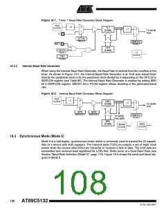
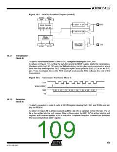
Figure 18-3. Serial I/O Port Block Diagram (Mode 0)
SCON.6
SCON.7
SM1
SM0
SBUF Tx SR
SBUF Rx SR
RXD
Mode Decoder
M3 M2 M1 M0
Mode
Controller
Baud Rate
Controller
TI
SCON.1
RI
SCON.0
TXD
18.3.1
Transmission
(Mode 0)
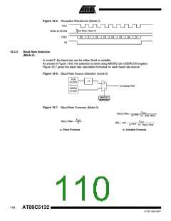
To start a transmission mode 0, write to SCON register clearing Bits SM0, SM1.
As shown in Figure 18-4, writing the byte to transmit to SBUF register starts the transmission.
Hardware shifts the LSB (D0) onto the RXD pin during the first clock cycle composed of a high
level then low level signal on TXD. During the eighth clock cycle the MSB (D7) is on the RXD
pin. Then, hardware drives the RXD pin high and asserts TI to indicate the end of the
transmission.
Figure 18-4. Transmission Waveforms (Mode 0)
TXD
Write to SBUF
RXD
TI
D0
D1
D2
D3
D4
D5
D6
D7
18.3.2
Reception
(Mode 0)
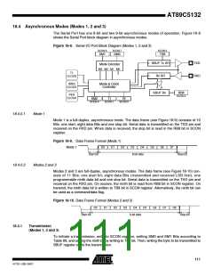
To start a reception in mode 0, write to SCON register clearing SM0, SM1 and RI Bits and set-
ting the REN bit.
As shown in Figure 18-5, Clock is pulsed and the LSB (D0) is sampled on the RXD pin. The D0
bit is then shifted into the shift register. After eight sampling, the MSB (D7) is shifted into the shift
register, and hardware asserts RI bit to indicate a completed reception. Software can then read
the received byte from SBUF register.
109
4173E–USB–09/07

 ATMEL [ ATMEL ]