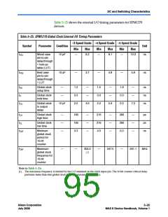
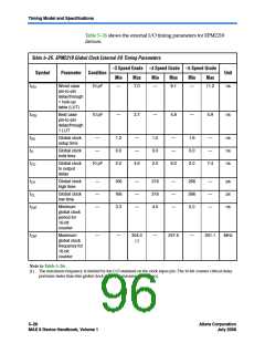
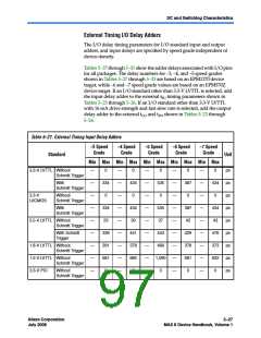
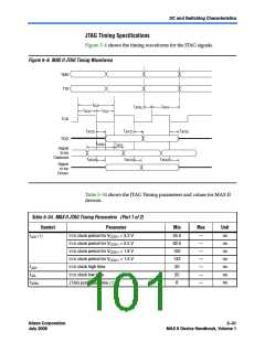
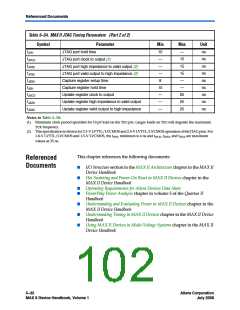
DC and Switching Characteristics
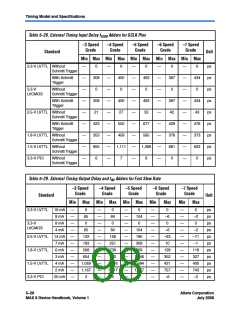
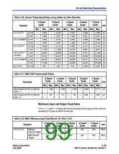
Table 5–30. External Timing Output Delay and tOD Adders for Slow Slew Rate
–3 Speed
Grade
–4 Speed
Grade
–5 Speed
Grade
–6 Speed
Grade
–7 Speed
Grade
Standard
Unit
Min
Max
Min
Max
Min
Max
Min Max Min Max
3.3-V LVTTL
16 mA
8 mA
—
—
—
—
—
—
—
—
—
—
—
7,064
7,946
—
—
—
—
—
—
—
—
—
—
—
6,745
7,627
—
—
—
—
—
—
—
—
—
—
—
6,426
7,308
6,426
7,308
9,796
10,910
22,289
24,093
38,085
40,692
418
—
—
—
—
—
—
—
—
—
—
—
5,966
6,541
5,966
6,541
9,141
9,861
21,811
23,081
39,121
40,631
6,644
—
—
—
—
—
—
—
—
—
—
—
5,992
6,570
5,992
6,570
9,154
9,874
ps
ps
ps
ps
ps
ps
3.3-V LVCMOS 8 mA
4 mA
7,064
6,745
7,946
7,627
2.5-V LVTTL
14 mA
7 mA
6 mA
3 mA
10,434
11,548
22,927
24,731
38,723
41,330
261
10,115
11,229
22,608
24,412
38,404
41,011
339
1.8-V LVTTL /
LVCMOS
21,854 ps
23,034 ps
39,124 ps
40,634 ps
1.5-V LVCMOS 4 mA
2 mA
3.3-V PCI
20 mA
6,627
ps
Table 5–31. MAX II IOE Programmable Delays
–3 Speed
Grade
–4 Speed
Grade
–5 Speed
Grade
–6 Speed
Grade
–7 Speed
Grade
Parameter
Unit
Min Max Min Max Min Max Min Max Min Max
Input Delay from Pin to Internal
Cells = 1
—
1,225
—
1,592
—
1,960
—
1,858
—
2,171 ps
Input Delay from Pin to Internal
Cells = 0
—
89
—
115
—
142
—
569
—
609 ps
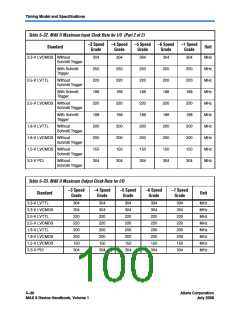
Maximum Input and Output Clock Rates
Tables 5–32 and 5–33 show the maximum input and output clock rates for
standard I/O pins in MAX II devices.
Table 5–32. MAX II Maximum Input Clock Rate for I/O (Part 1 of 2)
–3 Speed
Grade
–4 Speed
Grade
–5 Speed
Grade
–6 Speed
Grade
–7 Speed
Grade
Standard
Unit
3.3-V LVTTL
Without
304
304
304
304
304
MHz
Schmitt Trigger
With Schmitt
250
250
250
250
250
MHz
Trigger
Altera Corporation
July 2008
5–29
MAX II Device Handbook, Volume 1

 ALTERA [ ALTERA CORPORATION ]