DC and Switching Characteristics
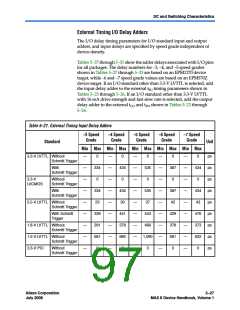
External Timing I/O Delay Adders
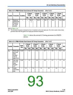
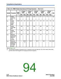
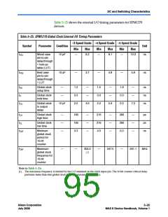
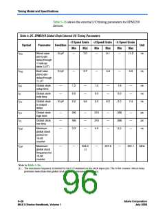
The I/O delay timing parameters for I/O standard input and output
adders, and input delays are specified by speed grade independent of
device density.
Tables 5–27 through 5–31 show the adder delays associated with I/O pins
for all packages. The delay numbers for –3, –4, and –5 speed grades
shown in Tables 5–27 through 5–33 are based on an EPM1270 device
target, while –6 and –7 speed grade values are based on an EPM570Z
device target. If an I/O standard other than 3.3-V LVTTL is selected, add
the input delay adder to the external tSU timing parameters shown in
Tables 5–23 through 5–26. If an I/O standard other than 3.3-V LVTTL
with 16 mA drive strength and fast slew rate is selected, add the output
delay adder to the external tCO and tPD shown in Tables 5–23 through
5–26.
Table 5–27. External Timing Input Delay Adders
–3 Speed –4 Speed
–5 Speed
Grade
–6 Speed
Grade
–7 Speed
Grade
Grade Grade
Standard
Unit
Min Max Min Max Min Max Min Max Min Max
3.3-V LVTTL Without
—
—
—
—
—
—
—
—
—
0
—
—
—
—
—
—
—
—
—
0
—
—
—
—
—
—
—
—
—
0
535
0
—
—
—
—
—
—
—
—
—
0
—
—
—
—
—
—
—
—
—
0
ps
ps
ps
ps
ps
ps
ps
ps
ps
Schmitt Trigger
With
Schmitt Trigger
334
0
434
0
387
0
434
0
3.3-V
Without
LVCMOS
Schmitt Trigger
With
Schmitt Trigger
334
23
434
30
535
37
387
42
434
43
2.5-V LVTTL Without
Schmitt Trigger
With Schmitt
Trigger
339
291
681
0
441
378
885
0
543
466
1,090
0
429
378
681
0
476
373
622
0
1.8-V LVTTL Without
Schmitt Trigger
1.5-V LVTTL Without
Schmitt Trigger
3.3-V PCI
Without
Schmitt Trigger
Altera Corporation
July 2008
5–27
MAX II Device Handbook, Volume 1

 ALTERA [ ALTERA CORPORATION ]