DC and Switching Characteristics
JTAG Timing Specifications
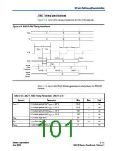
Figure 5–6 shows the timing waveforms for the JTAG signals.
Figure 5–6. MAX II JTAG Timing Waveforms
TMS
TDI
t
JCP
t
t
JPH
JPSU
t
t
JCL
JCH
TCK
TDO
t
t
t
JPXZ
JPZX
JPCO
t
t
JSSU
JSH
Signal
to be
Captured
t
t
t
JSXZ
JSZX
JSCO
Signal
to be
Driven
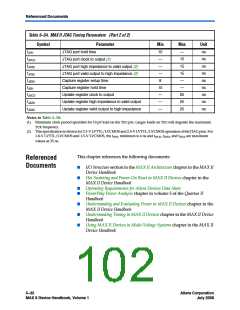
Table 5–34 shows the JTAG Timing parameters and values for MAX II
devices.
Table 5–34. MAX II JTAG Timing Parameters (Part 1 of 2)
Symbol
Parameter
TCKclock period for VCCIO1 = 3.3 V
TCKclock period for VCCIO1 = 2.5 V
TCKclock period for VCCIO1 = 1.8 V
TCKclock period for VCCIO1 = 1.5 V
TCKclock high time
Min
55.5
62.5
100
143
20
Max
—
Unit
ns
ns
ns
ns
ns
ns
ns
tJCP (1)
—
—
—
tJCH
tJCL
—
TCKclock low time
20
—
tJPSU
8
—
JTAG port setup time (2)
Altera Corporation
July 2008
5–31
MAX II Device Handbook, Volume 1

 ALTERA [ ALTERA CORPORATION ]