Referenced Documents
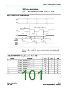
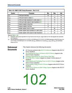
Table 5–34. MAX II JTAG Timing Parameters (Part 2 of 2)
Symbol
Parameter
Min
10
—
—
—
8
Max
—
Unit
ns
ns
ns
ns
ns
ns
ns
ns
ns
tJPH
JTAG port hold time
tJPCO
tJPZX
tJPXZ
tJSSU
tJSH
15
15
15
—
JTAG port clock to output (2)
JTAG port high impedance to valid output (2)
JTAG port valid output to high impedance (2)
Capture register setup time
Capture register hold time
10
—
—
—
—
tJSCO
tJSZX
tJSXZ
Update register clock to output
25
25
25
Update register high impedance to valid output
Update register valid output to high impedance
Notes to Table 5–34:
(1) Minimum clock period specified for 10 pF load on the TDOpin. Larger loads on TDOwill degrade the maximum
TCKfrequency.
(2) This specification is shown for 3.3-V LVTTL/LVCMOS and 2.5-V LVTTL/LVCMOS operation of the JTAG pins. For
1.8-V LVTTL/LVCMOS and 1.5-V LVCMOS, the tJPSU minimum is 6 ns and tJPCO, tJPZX, and tJPXZ are maximum
values at 35 ns.
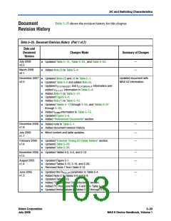
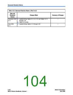
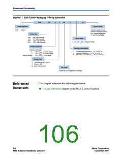
This chapter references the following documents:
Referenced
Documents
■
■
I/O Structure section in the MAX II Architecture chapter in the MAX II
Device Handbook
Hot Socketing and Power-On Reset in MAX II Devices chapter in the
MAX II Device Handbook
■
■
Operating Requirements for Altera Devices Data Sheet
PowerPlay Power Analysis chapter in volume 3 of the Quartus II
Handbook
■
■
■
Understanding and Evaluating Power in MAX II Devices chapter in the
MAX II Device Handbook
Understanding Timing in MAX II Devices chapter in the MAX II Device
Handbook
Using MAX II Devices in Multi-Voltage Systems chapter in the MAX II
Device Handbook
5–32Core Version a.b.c variable
Altera Corporation
MAX II Device Handbook, Volume 1
July 2008

 ALTERA [ ALTERA CORPORATION ]