DC and Switching Characteristics
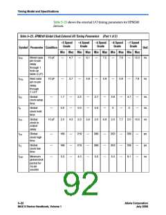
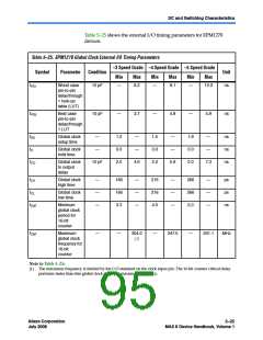
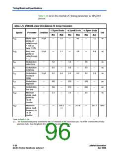
Table 5–25 shows the external I/O timing parameters for EPM1270
devices.
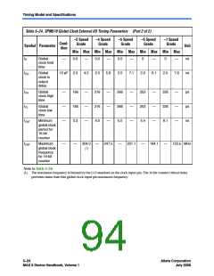
Table 5–25. EPM1270 Global Clock External I/O Timing Parameters
–3 Speed Grade –4 Speed Grade –5 Speed Grade
Symbol
Parameter
Condition
Unit
Min
Max
Min
Max
Min
Max
tPD1
Worst case
pin-to-pin
10 pF
—
6.2
—
8.1
—
10.0
ns
delaythrough
1 look-up
table (LUT)
tPD2
Best case
pin-to-pin
delaythrough
1 LUT
10 pF
—
3.7
—
4.8
—
5.9
ns
tSU
tH
Global clock
setup time
—
—
1.2
0.0
2.0
—
—
1.5
0.0
2.0
—
—
1.9
0.0
2.0
—
—
ns
ns
ns
Global clock
hold time
tCO
Global clock
to output
delay
10 pF
4.6
5.9
7.3
tCH
tCL
Global clock
high time
—
—
—
166
166
3.3
—
—
—
216
216
4.0
—
—
—
266
266
5.0
—
—
—
ps
ps
ns
Global clock
low time
tCNT
Minimum
global clock
period for
16-bit
counter
fCNT
Maximum
global clock
frequency for
16-bit
—
—
304.0
(1)
—
247.5
—
201.1
MHz
counter
Note to Table 5–25:
(1) The maximum frequency is limited by the I/O standard on the clock input pin. The 16-bit counter critical delay
performs faster than this global clock input pin maximum frequency.
Altera Corporation
July 2008
5–25
MAX II Device Handbook, Volume 1

 ALTERA [ ALTERA CORPORATION ]