DC and Switching Characteristics
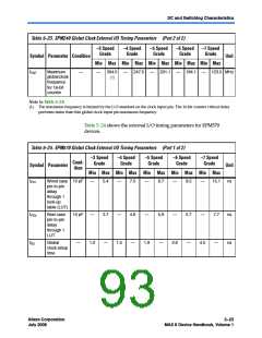
Table 5–23. EPM240 Global Clock External I/O Timing Parameters (Part 2 of 2)
–3 Speed
Grade
–4 Speed
Grade
–5 Speed
Grade
–6 Speed
Grade
–7 Speed
Grade
Symbol Parameter Condition
Unit
Min Max Min Max Min Max Min Max Min Max
fCNT
Maximum
globalclock
frequency
for 16-bit
counter
—
—
304.0
(1)
—
247.5
—
201.1
—
184.1
—
123.5 MHz
Note to Table 5–23:
(1) The maximum frequency is limited by the I/O standard on the clock input pin. The 16-bit counter critical delay
performs faster than this global clock input pin maximum frequency.
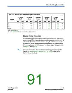
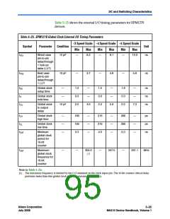
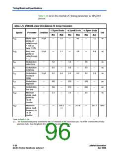
Table 5–24 shows the external I/O timing parameters for EPM570
devices.
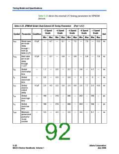
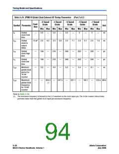
Table 5–24. EPM570 Global Clock External I/O Timing Parameters (Part 1 of 2)
–3 Speed
Grade
–4 Speed
Grade
–5 Speed
Grade
–6 Speed
Grade
–7 Speed
Grade
Cond-
ition
Symbol Parameter
Unit
Min Max Min Max Min Max Min Max Min Max
tPD1
Worst case 10 pF
pin-to-pin
—
5.4
—
7.0
—
8.7
—
9.5
—
15.1
ns
delay
through 1
look-up
table (LUT)
tPD2
Best case
pin-to-pin
delay
through 1
LUT
10 pF
—
3.7
—
—
4.8
—
—
5.9
—
—
5.7
—
—
7.7
—
ns
ns
tSU
Global
—
1.2
1.5
1.9
2.6
4.5
clock setup
time
Altera Corporation
July 2008
5–23
MAX II Device Handbook, Volume 1

 ALTERA [ ALTERA CORPORATION ]