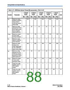
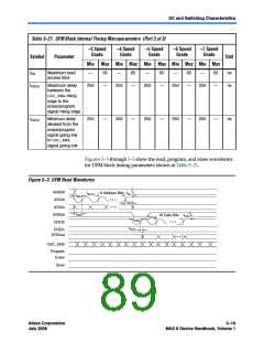
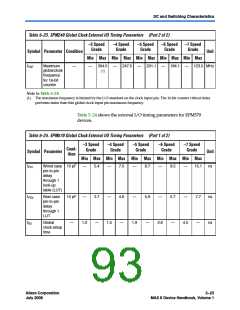
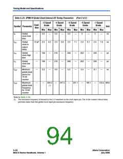
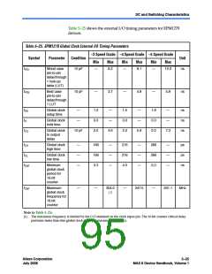
Timing Model and Specifications
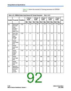
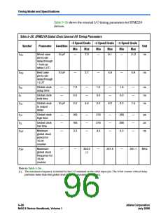
Table 5–23 shows the external I/O timing parameters for EPM240
devices.
Table 5–23. EPM240 Global Clock External I/O Timing Parameters (Part 1 of 2)
–3 Speed
Grade
–4 Speed
Grade
–5 Speed
Grade
–6 Speed
Grade
–7 Speed
Grade
Symbol Parameter Condition
Unit
Min Max Min Max Min Max Min Max Min Max
tPD1
Worst case
pin-to-pin
delay
through 1
look-up
10 pF
10 pF
—
4.7
—
6.1
—
7.5
—
7.9
—
12.0
ns
table (LUT)
tPD2
Best case
pin-to-pin
delay
—
3.7
—
4.8
—
5.9
—
5.8
—
7.8
ns
through
1 LUT
tSU
Global
clock setup
time
—
—
1.7
0.0
2.0
—
—
2.2
0.0
2.0
—
—
2.7
0.0
2.0
—
—
2.8
0
—
—
4.7
0
—
—
ns
ns
ns
tH
Global
clock hold
time
tCO
Global
clock to
output
delay
10 pF
4.3
5.6
6.9
2.0
7.7
2.0 10.5
tCH
Global
clock high
time
—
—
—
166
166
3.3
—
—
—
216
216
4.0
—
—
—
266
266
5.0
—
—
—
253
253
5.4
—
—
—
335
335
8.1
—
—
—
ps
ps
ns
tCL
Global
clock low
time
tCNT
Minimum
globalclock
period for
16-bit
counter
5–22Core Version a.b.c variable
MAX II Device Handbook, Volume 1
Altera Corporation
July 2008

 ALTERA [ ALTERA CORPORATION ]