Arria GX Architecture
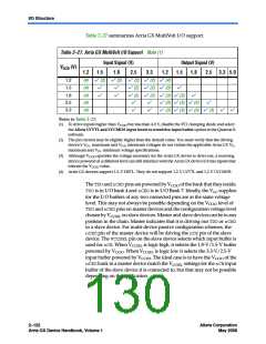
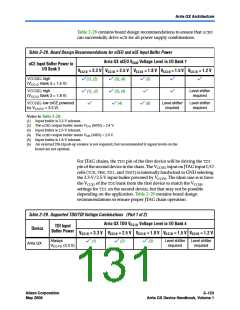
Table 2–28 contains board design recommendations to ensure that nCEO
can successfully drive nCEfor all power supply combinations.
Table 2–28. Board Design Recommendations for nCEO and nCE Input Buffer Power
Arria GX nCEO VCCIO Voltage Level in I/O Bank 7
nCE Input Buffer Power in
I/O Bank 3
VCCIO = 3.3 V VCCIO = 2.5 V VCCIO = 1.8 V VCCIO = 1.5 V VCCIO = 1.2 V
VCCSELhigh
(VCCIO Bank 3 = 1.5 V)
v(1), (2)
v (1), (2)
v
v (3), (4)
v (3), (4)
v (4)
v (5)
v
v
v
v
Level shifter
required
VCCSELhigh
(VCCIO Bank 3 = 1.8 V)
Level shifter
required
Level shifter
required
VCCSELlow (nCE powered
by VCCPD = 3.3 V)
v (6)
Notes to Table 2–28:
(1) Input buffer is 3.3-V tolerant.
(2) The nCEOoutput buffer meets VO H (MIN) = 2.4 V.
(3) Input buffer is 2.5-V tolerant.
(4) The nCEOoutput buffer meets VOH (MIN) = 2.0 V.
(5) Input buffer is 1.8-V tolerant.
(6) An external 250-Ωpull-up resistor is not required, but recommended if signal levels on the
board are not optimal.
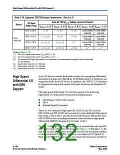
For JTAG chains, the TDOpin of the first device will be driving the TDI
pin of the second device in the chain. The VCCSEL input on JTAG input I/O
cells (TCK, TMS, TDI, and TRST) is internally hardwired to GND selecting
the 3.3-V/2.5-V input buffer powered by VCCPD. The ideal case is to have
the VCCIO of the TDObank from the first device to match the VCCSEL
settings for TDIon the second device, but that may not be possible
depending on the application. Table 2–29 contains board design
recommendations to ensure proper JTAG chain operation.
Table 2–29. Supported TDO/TDI Voltage Combinations (Part 1 of 2)
Arria GX TDO VCCIO Voltage Level in I/O Bank 4
TDI Input
Buffer Power
Device
VCCIO = 3.3 V VCCI O = 2.5 V VCCIO = 1.8 V VCCI O = 1.5 V VCCIO = 1.2 V
Always
VCCPD (3.3 V)
Level shifter
required
Level shifter
required
v (1)
v (2)
v (3)
Arria GX
Altera Corporation
May 2008
2–123
Arria GX Device Handbook, Volume 1

 ALTERA [ ALTERA CORPORATION ]