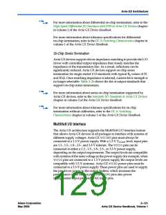
I/O Structure
Table 2–26 shows the Arria GX on-chip termination support per I/O
bank.
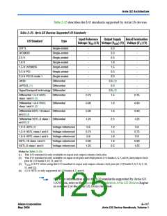
Table 2–26. On-Chip Termination Support by I/O Banks
Top and Bottom Banks
(3, 4, 7, 8)
On-Chip Termination Support
I/O Standard Support
Left Bank (1, 2)
3.3-V LVTTL
v
v
v
v
v
v
v
v
v
v
v
v
v
v
v
v
v
v
v
v
v
v
v
v
v
3.3-V LVCMOS
2.5-V LVTTL
2.5-V LVCMOS
1.8-V LVTTL
1.8-V LVCMOS
1.5-V LVTTL
1.5-V LVCMOS
SSTL-2 class I and II
SSTL-18 class I
SSTL-18 class II
1.8-V HSTL class I
1.8-V HSTL class II
1.5-V HSTL class I
1.2-V HSTL
Series termination
v
v
LVDS
v
v
Differential termination (1)
HyperTransport technology
Note to Table 2–26:
(1) Clock pins CLK1and CLK3, and pins FPLL[7..8]CLKdo not support differential on-chip termination. Clock pins
CLK0and CLK2, do support differential on-chip termination. Clock pins in the top and bottom banks (CLK[4..7,
12..15]) do not support differential on-chip termination.
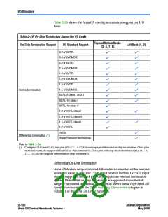
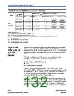
Differential On-Chip Termination
Arria GX devices support internal differential termination with a nominal
resistance value of 100 Ωfor LVDS input receiver buffers. LVPECL input
signals (supported on clock pins only) require an external termination
resistor. Differential on-chip termination is supported across the full
range of supported differential data rates as shown in the High-Speed I/O
Specifications section of the DC & Switching Characteristics chapter in
volume 1 of the Arria GX Device Handbook.
2–120
Altera Corporation
May 2008
Arria GX Device Handbook, Volume 1

 ALTERA [ ALTERA CORPORATION ]