I/O Structure
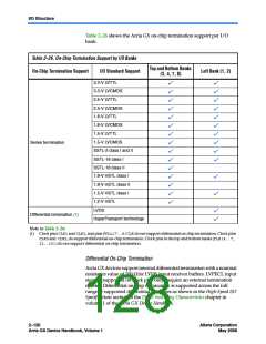
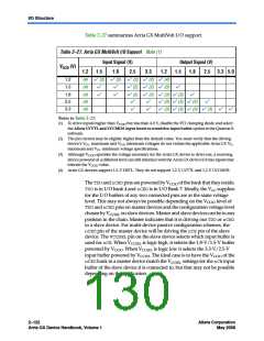
Table 2–27 summarizes Arria GX MultiVolt I/O support.
Table 2–27. Arria GX MultiVolt I/O Support Note (1)
Input Signal (V)
1.8 2.5
Output Signal (V)
VCCIO (V)
1.2
1.5
3.3
1.2
1.5
1.8
2.5
3.3 5.0
1.2
1.5
1.8
2.5
3.3
(4) v (2) v (2) v (2) v (2) v (4)
(4)
(4)
(4)
(4)
v
v
v
v
v (2) v (2) v (3)
v
v (2) v (2) v (3) v (3)
v
v
v
v
v
v (3) v (3) v (3)
v
v (3) v (3) v (3) v (3)
v
v
Notes to Table 2–27:
(1) To drive inputs higher than VCCIO but less than 4.0 V, disable the PCI clamping diode and select
the Allow LVTTL and LVCMOS input levels to overdrive input buffer option in the Quartus II
software.
(2) The pin current may be slightly higher than the default value. You must verify that the driving
device’s VOL maximum and VO H minimum voltages do not violate the applicable Arria GX VIL
maximum and VIH minimum voltage specifications.
(3) Although VCCIO specifies the voltage necessary for the Arria GX device to drive out, a receiving
device powered at a different level can still interface with the Arria GX device if it has inputs that
tolerate the VCCIO value.
(4) Arria GX devices support 1.2-V HSTL. They do not support 1.2-V LVTTL and 1.2-V LVCMOS.
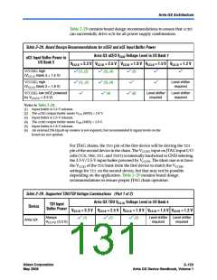
The TDOand nCEOpins are powered by VCCIO of the bank that they reside.
TDOis in I/O bank 4 and nCEOis in I/O Bank 7. Ideally, the VCC supplies
for the I/O buffers of any two connected pins are at the same voltage
level. This may not always be possible depending on the VCCIO level of
TDOand nCEOpins on master devices and the configuration voltage level
chosen by VCCSEL on slave devices. Master and slave devices can be in any
position in the chain. Master indicates that it is driving out TDOor nCEO
to a slave device. For multi-device passive configuration schemes, the
nCEOpin of the master device will be driving the nCEpin of the slave
device. The VCCSELpin on the slave device selects which input buffer is
used for nCE. When VCCSEL is logic high, it selects the 1.8-V/1.5-V buffer
powered by VCCIO. When VCCSEL is logic low it selects the 3.3-V/2.5-V
input buffer powered by VCCPD. The ideal case is to have the VCCIO of the
nCEObank in a master device match the VCCSEL settings for the nCEinput
buffer of the slave device it is connected to, but that may not be possible
depending on the application.
2–122
Arria GX Device Handbook, Volume 1
Altera Corporation
May 2008

 ALTERA [ ALTERA CORPORATION ]