Arria GX Architecture
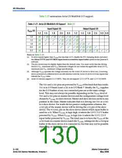
Each I/O bank has its own VCCIOpins. A single device can support
1.5-, 1.8-, 2.5-, and 3.3-V interfaces; each bank can support a different
VCCIO level independently. Each bank also has dedicated VREFpins to
support the voltage-referenced standards (such as SSTL-2).
Each I/O bank can support multiple standards with the same VCCIO for
input and output pins. Each bank can support one VREF voltage level. For
example, when VCCIO is 3.3 V, a bank can support LVTTL, LVCMOS, and
3.3-V PCI for inputs and outputs.
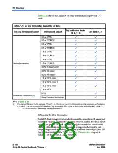
On-Chip Termination
Arria GX devices provide differential (for the LVDS technology I/O
standard) and series on-chip termination to reduce reflections and
maintain signal integrity. There is no calibration support for these on-chip
termination resistors. On-chip termination simplifies board design by
minimizing the number of external termination resistors required.
Termination can be placed inside the package, eliminating small stubs
that can still lead to reflections.
Arria GX devices provide two types of termination:
■
■
Differential termination (RD)
Series termination (RS)
Altera Corporation
May 2008
2–119
Arria GX Device Handbook, Volume 1

 ALTERA [ ALTERA CORPORATION ]