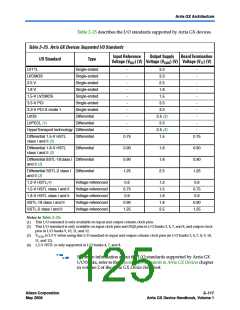
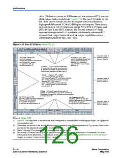
I/O Structure
Arria GX devices contain six I/O banks and four enhanced PLL external
clock output banks, as shown in Figure 2–78. The two I/O banks on the
left of the device contain circuitry to support source-synchronous,
high-speed differential I/O for LVDS inputs and outputs. These banks
support all Arria GX I/O standards except PCI or PCI-X I/O pins, and
SSTL-18 class II and HSTL outputs. The top and bottom I/O banks
support all single-ended I/O standards. Additionally, enhanced PLL
external clock output banks allow clock output capabilities such as
differential support for SSTL and HSTL.
Figure 2–78. Arria GX I/O Banks Notes (1), (2)
DQS ×8
DQS ×8
DQS ×8
DQS ×8
DQS ×8
DQS ×8
DQS ×8
DQS ×8
DQS ×8
PLL11
Bank 11
PLL5
PLL7 VREF0B3 VREF1B3 VREF2B3 VREF3B3 VREF4B3
Bank 3
VREF0B4 VREF1B4 VREF2B4 VREF3B4 VREF4B4
Bank 4
Bank 9
Transmitter: Bank 13
Receiver: Bank 13
REFCLK: Bank 13
This I/O bank supports LVDS
and LVPECL standards
for input clock operations. Differential HSTL
and differential SSTL standards
are supported for both input
and output operations. (3)
This I/O bank supports LVDS
and LVPECL standards for input clock
operation. Differential HSTL and
differential SSTL standards are
supported for both input and output
operations. (3)
I/O Banks 3, 4, 9, and 11 support all single-ended
I/O standards for both input and output operations.
All differential I/O standards are supported for both
input and output operations at I/O banks 9 and 11.
I/O banks 1 & 2 support LVTTL, LVCMOS,
2.5 V, 1.8 V, 1.5 V, SSTL-2, SSTL-18 class I,
LVDS, pseudo-differential SSTL-2 and pseudo-differential
SSTL-18 class I standards for both input and output
operations. HSTL, SSTL-18 class II,
pseudo-differential HSTL and pseudo-differential
SSTL-18 class II standards are only supported for
input operations. (4)
Transmitter: Bank 14
Receiver: Bank 14
REFCLK: Bank 14
PLL1
PLL2
I/O banks 7, 8, 10 and 12 support all single-ended I/O
standards for both input and output operations. All differential
I/O standards are supported for both input and output operations
at I/O banks 10 and 12.
This I/O bank supports LVDS
This I/O bank supports LVDS
and LVPECL standards for input clock operation.
Differential HSTL and differential
and LVPECL standards for input clock
operation. Differential HSTL and differential
SSTL standards are supported
Transmitter: Bank 15
Receiver: Bank 15
REFCLK: Bank 15
SSTL standards are supported
for both input and output operations. (3)
for both input and output operations. (3)
Bank 8
Bank 7
Bank 12
PLL12
Bank 10
PLL6
VREF4B8 VREF3B8 VREF2B8 VREF1B8 VREF0B8
VREF4B7 VREF3B7 VREF2B7 VREF1B7 VREF0B7
PLL8
DQS ×8
DQS ×8
DQS ×8
DQS ×8
DQS ×8
DQS ×8
DQS ×8
DQS ×8
DQS ×8
Notes to Figure 2–78:
(1) Figure 2–78 is a top view of the silicon die that corresponds to a reverse view for flip chip packages. It is a graphical
representation only.
(2) Depending on the size of the device, different device members have different numbers of VREF groups. Refer to the
pin list and the Quartus II software for exact locations.
(3) Banks 9 through 12 are enhanced PLL external clock output banks.
(4) Horizontal I/O banks feature SERDES and DPA circuitry for high-speed differential I/O standards. For more
information about differential I/O standards, refer to the High-Speed Differential I/O Interfaces in Arria GX Devices
chapter in volume 2 of the Arria GX Device Handbook.
2–118
Altera Corporation
May 2008
Arria GX Device Handbook, Volume 1

 ALTERA [ ALTERA CORPORATION ]