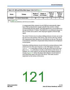
Arria GX Architecture
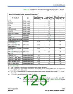
Table 2–25 describes the I/O standards supported by Arria GX devices.
Table 2–25. Arria GX Devices Supported I/O Standards
Input Reference
Voltage (VREF) (V) Voltage (VCCIO) (V) Voltage (VTT) (V)
Output Supply
BoardTermination
I/O Standard
Type
LVTTL
Single-ended
Single-ended
Single-ended
Single-ended
Single-ended
Single-ended
Single-ended
Differential
-
3.3
3.3
-
LVCMOS
-
-
2.5 V
-
2.5
-
1.8 V
-
1.8
-
1.5-V LVCMOS
3.3-V PCI
3.3-V PCI-X mode 1
LVDS
-
1.5
-
-
3.3
-
-
3.3
-
-
2.5 (3)
3.3
-
LVPECL (1)
Differential
-
-
-
-
HyperTransport technology Differential
2.5 (3)
1.5
Differential 1.5-V HSTL
Differential
0.75
0.75
class I and II (2)
Differential 1.8-V HSTL
class I and II (2)
Differential
0.90
0.90
1.25
1.8
1.8
2.5
0.90
0.90
1.25
DifferentialSSTL-18class I Differential
and II (2)
Differential SSTL-2 class I Differential
and II (2)
1.2-V HSTL(4)
Voltage-referenced
0.6
0.75
0.9
1.2
1.5
1.8
1.8
2.5
0.6
0.75
0.9
1.5-V HSTL class I and II
1.8-V HSTL class I and II
SSTL-18 class I and II
SSTL-2 class I and II
Voltage-referenced
Voltage-referenced
Voltage-referenced
Voltage-referenced
0.90
1.25
0.90
1.25
Notes to Table 2–25:
(1) This I/O standard is only available on input and output column clock pins.
(2) This I/O standard is only available on input clock pins and DQS pins in I/O banks 3, 4, 7, and 8, and output clock
pins in I/O banks 9, 10, 11, and 12.
(3) VCCIO is 3.3 V when using this I/O standard in input and output column clock pins (in I/O banks 3, 4, 7, 8, 9, 10,
11, and 12).
(4) 1.2-V HSTL is only supported in I/O banks 4, 7, and 8.
f
For more information about the I/O standards supported by Arria GX
I/O banks, refer to the Selectable I/O Standards in Arria GX Devices chapter
in volume 2 of the Arria GX Device Handbook.
Altera Corporation
May 2008
2–117
Arria GX Device Handbook, Volume 1

 ALTERA [ ALTERA CORPORATION ]