I/O Structure
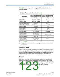
Bus-hold circuitry also pulls undriven pins away from the input
threshold voltage where noise can cause unintended high-frequency
switching. You can select this feature individually for each I/O pin. The
bus-hold output drives no higher than VCCIO to prevent overdriving
signals. If the bus-hold feature is enabled, the programmable pull-up
option cannot be used. Disable the bus-hold feature when the I/O pin has
been configured for differential signals.
Bus-hold circuitry uses a resistor with a nominal resistance (RBH) of
approximately 7 kΩto pull the signal level to the last-driven state. This
information is provided for each VCCIO voltage level. Bus-hold circuitry is
active only after configuration. When going into user mode, the bus-hold
circuit captures the value on the pin present at the end of configuration.
f
For the specific sustaining current driven through this resistor and
overdrive current used to identify the next-driven input level, refer to
the DC & Switching Characteristics chapter in volume 1 of the Arria GX
Device Handbook.
Programmable Pull-Up Resistor
Each Arria GX device I/O pin provides an optional programmable
pull-up resistor during user mode. If you enable this feature for an I/O
pin, the pull-up resistor (typically 25 kΩ) holds the output to the VCCIO
level of the output pin’s bank.
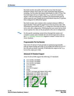
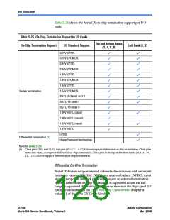
Advanced I/O Standard Support
Arria GX device IOEs support the following I/O standards:
■
■
■
■
■
■
■
■
■
■
■
■
■
■
■
■
■
3.3-V LVTTL/LVCMOS
2.5-V LVTTL/LVCMOS
1.8-V LVTTL/LVCMOS
1.5-V LVCMOS
3.3-V PCI
3.3-V PCI-X mode 1
LVDS
LVPECL (on input and output clocks only)
Differential 1.5-V HSTL class I and II
Differential 1.8-V HSTL class I and II
Differential SSTL-18 class I and II
Differential SSTL-2 class I and II
1.2-V HSTL class I and II
1.5-V HSTL class I and II
1.8-V HSTL class I and II
SSTL-2 class I and II
SSTL-18 class I and II
2–116
Arria GX Device Handbook, Volume 1
Altera Corporation
May 2008

 ALTERA [ ALTERA CORPORATION ]