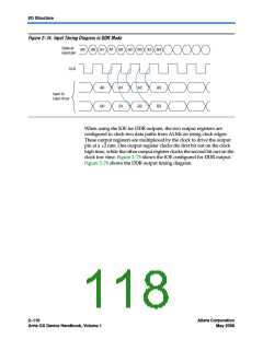
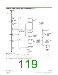
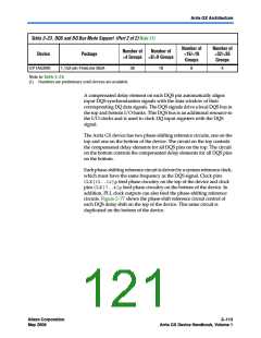
I/O Structure
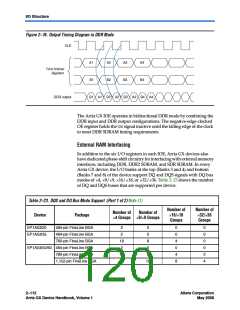
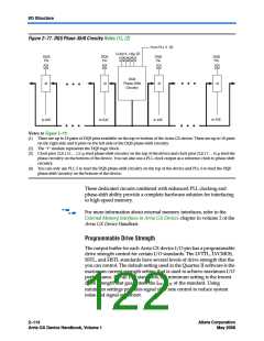
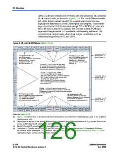
Figure 2–77. DQS Phase-Shift Circuitry Notes (1), (2)
From PLL 5 (4)
CLK[15..12]p (3)
DQS
Pin
DQS
Pin
DQS
Pin
DQS
Pin
DQS
Δt
Δt
Δt
Δt
Phase-Shift
Circuitry
to IOE
to IOE
to IOE
to IOE
Notes to Figure 2–77:
(1) There are up to 18 pairs of DQS pins available on the top or bottom of the Arria GX device. There are up to 10 pairs
on the right side and 8 pairs on the left side of the DQS phase-shift circuitry.
(2) The “t” module represents the DQS logic block.
(3) Clock pins CLK[15..12]pfeed phase-shift circuitry on the top of the device and clock pins CLK[7..4]pfeed the
phase circuitry on the bottom of the device. You can also use a PLL clock output as a reference clock to phase shift
circuitry.
(4) You can only use PLL 5 to feed the DQS phase-shift circuitry on the top of the device and PLL 6 to feed the DQS
phase-shift circuitry on the bottom of the device.
These dedicated circuits combined with enhanced PLL clocking and
phase-shift ability provide a complete hardware solution for interfacing
to high-speed memory.
f
For more information about external memory interfaces, refer to the
External Memory Interfaces in Arria GX Devices chapter in volume 2 of the
Arria GX Device Handbook.
Programmable Drive Strength
The output buffer for each Arria GX device I/O pin has a programmable
drive strength control for certain I/O standards. The LVTTL, LVCMOS,
SSTL, and HSTL standards have several levels of drive strength that the
you can control. The default setting used in the Quartus II software is the
maximum current strength setting that is used to achieve maximum I/O
performance. For all I/O standards, the minimum setting is the lowest
drive strength that guarantees the IOH/IOL of the standard. Using
minimum settings provides signal slew rate control to reduce system
noise and signal overshoot.
2–114
Arria GX Device Handbook, Volume 1
Altera Corporation
May 2008

 ALTERA [ ALTERA CORPORATION ]