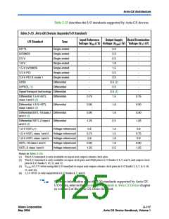
Arria GX Architecture
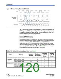
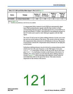
Table 2–23. DQS and DQ Bus Mode Support (Part 2 of 2) Note (1)
Number of
×16/×18
Groups
Number of
×32/×36
Groups
Number of
×4 Groups ×8/×9 Groups
Number of
Device
Package
EP1AGX90
1,152-pin FineLine BGA
36
18
8
4
Note to Table 2–23:
(1) Numbers are preliminary until devices are available.
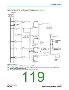
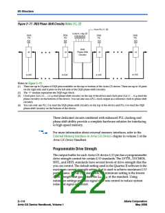
A compensated delay element on each DQS pin automatically aligns
input DQS synchronization signals with the data window of their
corresponding DQ data signals. The DQS signals drive a local DQS bus in
the top and bottom I/O banks. This DQS bus is an additional resource to
the I/O clocks and is used to clock DQ input registers with the DQS
signal.
The Arria GX device has two phase-shifting reference circuits, one on the
top and one on the bottom of the device. The circuit on the top controls
the compensated delay elements for all DQS pins on the top. The circuit
on the bottom controls the compensated delay elements for all DQS pins
on the bottom.
Each phase-shifting reference circuit is driven by a system reference clock,
which must have the same frequency as the DQS signal. Clock pins
CLK[15..12]pfeed phase circuitry on the top of the device and clock
pins CLK[7..4]pfeed phase circuitry on the bottom of the device. In
addition, PLL clock outputs can also feed the phase-shifting reference
circuits. Figure 2–77 shows the phase-shift reference circuit control of
each DQS delay shift on the top of the device. This same circuit is
duplicated on the bottom of the device.
Altera Corporation
May 2008
2–113
Arria GX Device Handbook, Volume 1

 ALTERA [ ALTERA CORPORATION ]