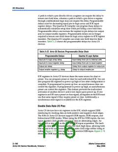
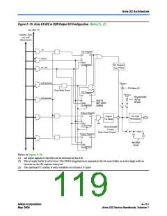
I/O Structure
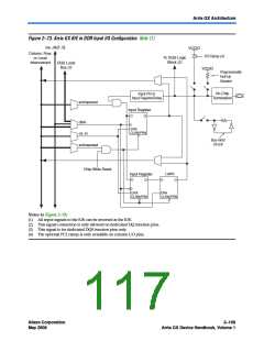
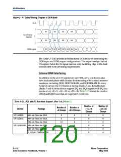
Figure 2–76. Output Timing Diagram in DDR Mode
CLK
A1
B1
A2
B2
A3
B3
A4
B4
From Internal
Registers
B1 A1 B2 A2 B3 A3 B4 A4
DDR output
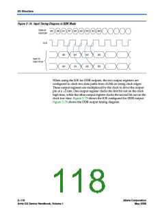
The Arria GX IOE operates in bidirectional DDR mode by combining the
DDR input and DDR output configurations. The negative-edge-clocked
OE register holds the OEsignal inactive until the falling edge of the clock
to meet DDR SDRAM timing requirements.
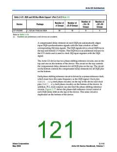
External RAM Interfacing
In addition to the six I/O registers in each IOE, Arria GX devices also
have dedicated phase-shift circuitry for interfacing with external memory
interfaces, including DDR, DDR2 SDRAM, and SDR SDRAM. In every
Arria GX device, the I/O banks at the top (Banks 3 and 4) and bottom
(Banks 7 and 8) of the device support DQ and DQS signals with DQ bus
modes of ×4, ×8/×9, ×16/×18, or ×32/×36. Table 2–23 shows the number
of DQ and DQS buses that are supported per device.
Table 2–23. DQS and DQ Bus Mode Support (Part 1 of 2) Note (1)
Number of
×16/×18
Groups
Number of
×32/×36
Groups
Number of
×4 Groups ×8/×9 Groups
Number of
Device
Package
EP1AGX20
EP1AGX35
484-pin FineLine BGA
484-pin FineLine BGA
780-pin FineLine BGA
2
2
0
0
0
0
4
0
4
8
0
0
0
0
0
4
18
2
8
EP1AGX50/60 484-pin FineLine BGA
780-pin FineLine BGA
0
18
36
8
1,152-pin FineLine BGA
18
2–112
Altera Corporation
May 2008
Arria GX Device Handbook, Volume 1

 ALTERA [ ALTERA CORPORATION ]