[AK4679]
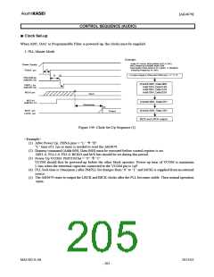
4. EXT Master Mode
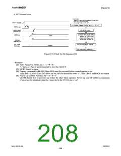
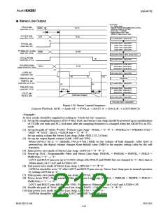
Example:
Audio I/F Format: MSB justified (ADC and DAC)
Input MCKI frequency: 256fs
Power Supply
Sampling Frequency: 44.1kHz
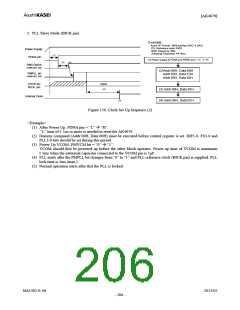
(1) Power Supply & PDN pin = “L” Æ “H”
(1)
PDNA pin
(4)
(2) MCKI input
PMVCM bit
(Addr:00H, D0)
(2)
(3)
(3)Addr:00H, Data:00H
Addr:03H, Data:F0H
Addr:04H, Data:02H
Addr:05H, Data02H
MCKI pin
Input
M/S bit
(Addr:04H, D1)
LRCK pin
BICK pin
BICK and LRCK output
(4) Addr:00H, Data:01H
Output
Figure 152. Clock Set Up Sequence (4)
<Example>
(1) After Power Up, PDNA pin = “L” Æ “H”.
“L” time of 1.5μs or more is needed to reset the AK4679.
(2) MCKI should be input.
(3) Dummy command (Addr:00H, Data:00H) must be executed before control register is set.
After DIF1-0, CM1-0 and FS3-0 bits are set, M/S bit should be set to “1”. Then LRCK and BICK are output.
(4) Power Up VCOM: PMVCM bit = “0” Æ “1”
VCOM should first be powered up before the other block operates. Power-up time of VCOM is maximum
1.5ms when the exterenal capacitor connected to the VCOM pin is 1μF.
MS1402-E-06
2013/02
- 208 -

 AKM [ ASAHI KASEI MICROSYSTEMS ]