[AK4679]
1. Grounding and Power Supply Decoupling
The AK4679 requires careful attention to power supply and grounding arrangements. AVDD, PVDD and SVDD are
usually supplied from the system’s analog supply, and DVDD, TVDDA, TVDDE and VDDE are supplied from the
system’s digital power supply. The power-up sequence between supplies (AVDD, PVDD, SVDD, DVDD, TVDDA,
TVDDE or VDDE) is not critical. PDNA and PDNE pins should be held “L” when power supplies are tuning on. PDNA
and PDNE pins are allowed to be “H” after all power supplies are applied and settled.
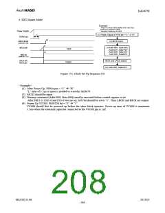
To avoid pop noise at receiver output, headphone outputs, speaker output and line outputs, the AK4679 should be
operated along the following recommended power-up/down sequence.
1) Power-up
- PDNA and PDNE pins should be held “L” when power supplies are turning on. The AK4679 can be reset by keeping
the PDNA pin “L” for 1.5μs or longer after all power supplies are applied and settled.
- In the case that the power supplies are separated in two or more groups, SVDD should be powered ON first.
2) Power-down
- Each of power supplies can be powered OFF after PDNA and PDNE pins are set to “L”.
- In the case that the power supplies are separated in two or more groups, SVDD should be powered OFF last.
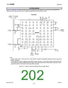
VSS1~5 of the AK4679 should be connected to the analog ground plane. System analog ground and digital ground should
be connected together near where the supplies are brought onto the printed circuit board. Decoupling capacitors should be
as near the AK4679 as possible. Especially, the small value ceramic capacitor is to be closest.
2. Voltage Reference
VCOM is a signal ground of this chip. A 1μF electrolytic capacitor attached to the VCOM pin eliminates the effects of
high frequency noise. No load current is allowed to be drawn from the VCOM pin. All signals, especially clocks, should
be kept away from the VCOM pin in order to avoid unwanted coupling into the AK4679.
3. Charge Pump
2.2μF±50% capacitors between the CPA to CNA pins, the CPB to CNB pins and the VEE to VSS5 pins should be low
ESR ceramic capacitors. These capacitors must be connected as close as possible to the pins. No load current may be
drawn from the VEE pin.
4. Analog Inputs
The input signal range scales with 1.0 x AVDD Vpp (typ) at MGNL=MGNR=0dB, AVDD=1.8V and single-ended input,
centered around the internal common voltage (typ. 0.47 x AVDD). The input signal must be AC coupled using a
capacitor. The cut-off frequency (fc) is 1/(2πRC).
5. Analog Outputs
Stereo Line outputs and Mono Receiver output are centered at typ. 0.8 x AVDD. Stereo line output (LOUT/ROUT pins)
must be AC –coupled using a capacitor. Receiver output (RCP/RCN pins) should be connected directly to a receiver.
Headphone outputs (HPL/HPR pin) are centered at 0V and should be directly connected to a headphone. Speaker output
is PWM output (Class-D) and it is not necessary to add an external filter such as LC filters.
MS1402-E-06
2013/02
- 204 -

 AKM [ ASAHI KASEI MICROSYSTEMS ]