[AK4679]
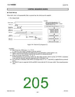
2. PLL Slave Mode (BICK pin)
Example:
Audio I/F Format : MSB justified (ADC & DAC)
PLL Reference clock: BICK
BICK frequency: 64fs
Power Supply
Sampling Frequency: 44.1kHz
(1)
PDNA pin
4fs of
(1) Power Supply & PDNA and PDNE pins = “L” Æ “H”
(2)
(3)
PMVCM bit
(Addr:00H, D0)
(2)Addr:00H, Data:00H
Addr:03H, Data:F3H
Addr:05H, Data:02H
PMPLL bit
(Addr:04H, D0)
LRCK pin
BICK pin
Input
(4)
(3) Addr:00H, Data:01H
(4) Addr:04H, Data:01H
Internal Clock
(5)
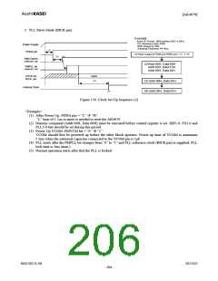
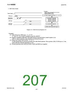
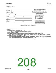
Figure 150. Clock Set Up Sequence (2)
<Example>
(1) After Power Up, PDNA pin = “L” Æ “H”.
“L” time of 1.5μs or more is needed to reset the AK4679.
(2) Dummy command (Addr:00H, Data:00H) must be executed before control register is set. DIF1-0, FS3-0 and
PLL3-0 bits should be set during this period.
(3) Power Up VCOM: PMVCM bit = “0” Æ “1”
VCOM should first be powered up before the other block operates. Power-up time of VCOM is maximum
1.5ms when the exterenal capacitor connected to the VCOM pin is 1μF.
(4) PLL starts after the PMPLL bit changes from “0” to “1” and PLL reference clock (BICK pin) is supplied. PLL
lock time is 2ms (max.).
(5) Normal operation starts after that the PLL is locked.
MS1402-E-06
2013/02
- 206 -

 AKM [ ASAHI KASEI MICROSYSTEMS ]