performed if the frame is a fill
frame.
between high and low for data
frames. This allows the link to
perform more extensive error
detection when the extra bit is
unused.
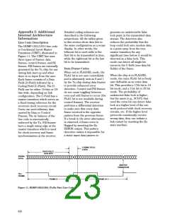
accomplished by applying a high
signal to EHCLKSEL and a
differential clock to STRBIN.
The Output Select block allows
the user to select between two
sets of differential high speed
serial outputs. This feature is
useful for loop back testing. If
LOOPEN is high, LOUT is enabled
and DOUT is disabled. If LOOPEN
is low, DOUT is enabled and
LOUT is disabled.
One of four frequency bands may
be selected by applying appropri-
ate inputs to DIV0 and DIV1. The
VCO or STRBIN frequency is
divided by N, where N is 1, 2, 4,
or 8 corresponding to the binary
number represented by DIV1,
DIV0. This divided version of the
VCO clock or STRBIN is used as
the serial rate clock and is
ACCMSB is the sign of the pre-
viously transmitted data. This is
used to determine which type of
FF1 should be sent. When
ACCMSB is low, FF1a is sent and
when ACCMSB is high, FF1b is
sent. This effectively drives the
accumulated offset of transmitted
bits back toward the balanced
state.
The active-low RST* input resets
the internal registers to a
balanced state. This pin should be
held low for at least five frame
rate clock cycles to ensure a
complete reset.
available as a differential signal at
the HCLK output.
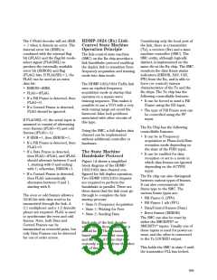
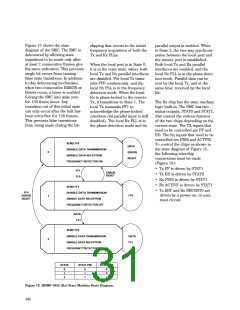
Tx Phase-Locked Loop
The block diagram of the
A clock generator block creates
all the clock signals required for
the chip. Depending on M20SEL,
STRBOUT is either HCLK/20 or
HCLK/24. If MDFSEL is low, then
STRBOUT is a phase-locked
version of STRBIN. If MDFSEL is
high, STRBOUT is twice the
frequency of STRBIN.
transmitter phase-locked loop is
shown in Figure 12. It consists of
a sequential frequency detector,
loop filter, VCO, clock generation
circuitry, and a lock indicator.
The outputs of the frequency
detector pass through a charge
pump filter that controls the
center frequency of the VCO.
These outputs also go to the VCO
directly to effectively add a zero
in the loop response. An external
high-speed clock can be used
instead of the VCO clock. This is
The Data Field and Control Field
are encoded depending on ED,
FF, DAV*, CAV*, FLAG,
FLAGSEL, M20SEL as well as two
internally generated signals, O/E
and ACCMSB.
When FLAGSEL is high, O/E is
equivalent to FLAG. This is
equivalent to adding an additional
bit to the data field. When
The lock detect circuit samples
STRBIN with phase shifted
versions of STRBOUT. If the
samples are not the proper
values, the LOCKED signal goes
low and stays low for at least two
frames.
FLAGSEL is low, O/E alternates
STRBIN
FREQ
VCO
FILTER
DETECT
INTERNAL CLOCKS
0
M20SEL
MDFSEL
CLOCK
GENERATOR
DIV N
1
STRBIN
EHCLKSEL
LOCK
DETECT
STRBOUT
HCLK
DIV0
DIV1
LOCKED
Figure 12. HDMP-1022 (Tx) Phase-Locked Loop.
642

 AGILENT [ AGILENT TECHNOLOGIES, LTD. ]