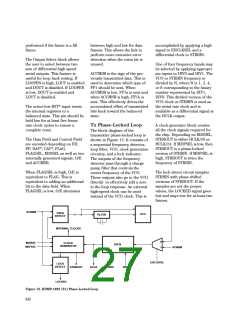
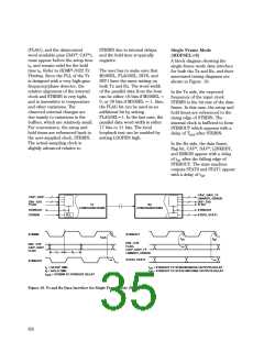
Figure 15 shows the state
slipping that occurs in the initial
frequency acquisition of both the
Tx and Rx PLLs.
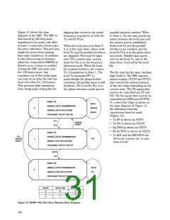
parallel output is enabled. When
in State 2, the two-way synchroni-
zation between the local port and
the remote port is established.
Both local Tx and Rx parallel
interfaces are enabled, and the
local Rx PLL is in the phase detec-
tion mode. Parallel data can be
sent by the local Tx, and at the
same time, received by the local
Rx.
diagram of the SMC. The SMC is
debounced by allowing state
transitions to be made only after
at least 2 consecutive frames give
the same indication. This prevents
single bit errors from causing
false state transitions. In addition
to this debouncing mechanism,
when two consecutive ERROR or
Resets occur, a timer is enabled
forcing the SMC into state zero
for 128 frame times. Any
transition out of this initial state
can only occur after the link has
been error-free for 128 frames.
This prevents false transitions
from being made during the bit-
When the local port is in State 0,
it is in the reset state, where both
local Tx and Rx parallel interfaces
are disabled. The local Tx trans-
mits FF0 continuously, and the
local Rx PLL is in the frequency
detection mode. When the local
Rx is phase-locked to the remote
Tx, it transitions to State 1. The
local Tx transmits FF1 to
The Rx chip has the state machine
logic built in. The SMC has two
status outputs, STAT0 and STAT1,
that control the various features
of the two chips depending on the
current state. The TX inputs that
need to be controlled are FF and
ED. The Rx inputs that need to be
controlled are FDIS and ACTIVE.
To control the chips as shown in
the state diagram of Figure 15,
the following interchip
acknowledge the phase-locked
condition (its parallel input is still
disabled). The local Rx PLL is in
the phase detection mode and its
SEND FF0
DATA
DISABLE DATA TRANSMISSION
DISABLE DATA RECEPTION
0
1
2
ERROR
RESET
connections must be made
(Figure 16):
FREQUENCY DETECTOR ON
• Tx FF is driven by STAT1
• Tx ED is driven by STAT0
• Rx FDIS is driven by STAT1
• Rx ACTIVE is driven by STAT1
• Tx RST and Rx SMCRST0 are
driven by a power-on, or user,
reset circuit.
FF1
FF0
ERROR
RESET
SEND FF1
FF0
ERROR
RESET
DISABLE DATA TRANSMISSION
ENABLE DATA RECEPTION
FREQUENCY DETECTOR OFF
FF0
DATA
FF1
SEND FF0
ENABLE DATA TRANSMISSION
ENABLE DATA RECEPTION
FREQUENCY DETECTOR OFF
DATA
FF1
STATE
STAT1 PIN
STAT0 PIN
0
0
1
0
1
2
0
1
1
Figure 15. HDMP-1024 (Rx) State Machine State Diagram.
646

 AGILENT [ AGILENT TECHNOLOGIES, LTD. ]