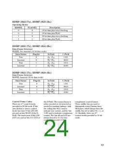
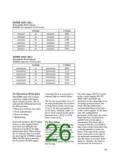
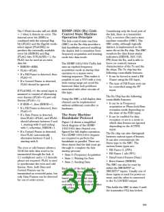
HDMP-1024 (Rx)
Detectable Error States
M20SEL Not Asserted (16 bit mode)
D-Field
C-Field
x00x
x11x
1100
1100
1010
0101
xxxxxxx
xxxxxxx
xxxxxxx
xxxxxxx
xxxxxxx
xxxxxxx
xx
xx
0x
11
xx
xx
xxxxxxx
xxxxxxx
xxxxxxx
xxxxxxx
xxxxxxx
xxxxxxx
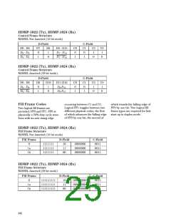
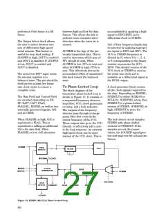
HDMP-1024 (Rx)
Detectable Error States
M20SEL Asserted (20 bit mode)
D-Field
C-Field
x00x
x11x
1100
1100
1010
0101
xxxxxxxxx
xxxxxxxxx
xxxxxxxxx
xxxxxxxxx
xxxxxxxxx
xxxxxxxxx
xx
xx
0x
11
xx
xx
xxxxxxxxx
xxxxxxxxx
xxxxxxxxx
xxxxxxxxx
xxxxxxxxx
xxxxxxxxx
Tx Operation Principles
indicating that it is now ready to
transmit data or control frames.
The data inputs, D0-D19, as well
as the control signals; ED, FF,
DAV*, CAV*, and FLAG are
latched in on the rising edge of an
internally generated frame rate
clock. The data field is then
encoded depending on the state
of the control signals. At the same
time, the coding field is
generated. At this point, the entire
frame has been constructed in
parallel form and its sign is
determined. This frame sign is
compared with the accumulated
sign of previously transmitted bits
to decide whether to invert the
frame. If the sign of the current
frame is the same as the sign of
the previously transmitted bits,
then the frame is inverted. If the
signs are opposite, the frame is
not inverted. No inversion is
The HDMP-1022 (Tx) is imple-
mented in a high performance
silicon bipolar process. The Tx
performs the following functions
for link operation:
• Phase lock to frame rate clock
• Clock multiplication
• Frame encoding
The Tx can accept either 16 or 17
bit wide parallel data and produce
a 20 bit frame. It also can accept
20 or 21 bit data and produce a
24 bit frame. Similarly, either 14
bit or 18 bit control words can be
transmitted in a 20 bit or 24 bit
frame respectively.
• Multiplexing
In normal operation, the Tx phase
locks to a user supplied frame
rate clock and multiplies the
frequency to produce the high
speed serial clock. When locked,
the Tx indicates that it is locked
by asserting the LOCKED output.
When the ED input is asserted,
the Tx asserts the RFD signal
Tx Encoding
A simplified block diagram of the
transmitter is shown in Figure 4.
The PLL/Clock Generator locks
onto the incoming frame rate (or
one-half frame rate) clock and
multiplies it up to the serial clock
rate. It also generates all the
internal clock signals required by
the Tx chip.
641

 AGILENT [ AGILENT TECHNOLOGIES, LTD. ]