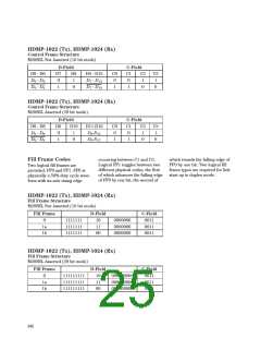
HDMP-1024 (Rx) Phase-
Locked Loop
frequency detector, however, can
only work with FF0 and FF1 and
it is necessary for the PLL
selecting the phase detector (by
setting FDIS=1) before receiving
any random data.
at a time. Every frame is
composed of a 16-bit or 20-bit
Data Field (D-Field) and a 4-bit
Control Field (C-Field). The C-
Field, C0-C3, together with the
two center bits of the D-Field (D9
and D10 for 20 bit mode, D7 and
D8 for 16 bit mode) are then
decoded by the C-Field decoder to
determine the content of the
frame. The D-Field decoder is
controlled by the outputs of the
C-Field decoder. If an inverted
Data Word or Control Word is
detected, the D-Field decoder will
automatically invert the D-Field
data. If a Control Frame is
detected, the D-Field decoder will
shift the bottom half of the D-
Field so that the outputs are at
pin D0 - D17 (if M20SEL =1) or at
pin D0 - D13 (if M20SEL =0). A
data Frame is detected by the
receiver when DAV = 1. A control
Frame is detected by the receiver
if CAV = 1. A Fill Frame is
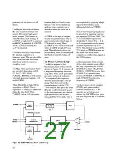
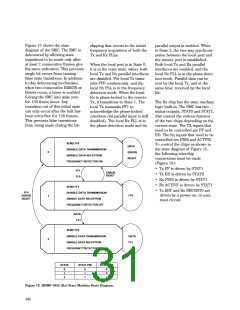
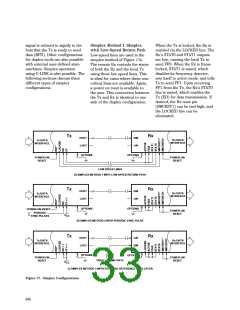
A more detailed block diagram for
the Rx phase-locked loop (PLL) is
shown in Figure 14. In the PLL,
the phase of the serial input, SIN,
is compared with synchronizing
signals from the internal clock
generator, using either a phase
detector or a frequency detector.
The frequency detector disable
signal, FDIS, selects which
detector to use. If synchronization
in a link is not yet established, the
HDMP-1022 (Tx) should send out
Fill Frame 0 (FF0) or Fill Frame 1
(FF1) to the remote Rx. By
setting FDIS=0, the Rx uses the
frequency detector to align its
internal clock with the rising edge
of FF0/FF1. Once frequency lock
is accomplished, FDIS can be set
to 1, then the PLL uses only the
phase detector for synchronization
adjustment and the Rx is ready to
receive data. Due to the narrow
frequency acquisition range of the
phase detector, the frequency
detector is used for internal
The output of the phase-
frequency detector is externally
available through pin PHI. An
external clock source can also be
used (through pin TCLK) by
setting TCLKSEL=1. To broaden
the usable frequency range of the
chip, there is a programmable
divider before the clock
generator. The VCO or TCLK
frequency can be divided by 1, 2,
4, 8 by setting DIV1, DIV0 = 00,
01, 10, 11 (see Operating Rate
Tables).
HDMP-1024 (Rx)
Decoding
In Figure 5, the frame
demultiplexer de-serializes the
recovered serial data from the
Input Sampler, and outputs the
resulting parallel data one frame
detected by the receiver if
DAV = 0 and CAV = 0.
frequency acquisition. The
FDIS
FREQ
0
1
PH1
SIN
PHASE
0
CLOCK GEN
DIV N
STRBOUT
VCO
1
FILTER
DIV0 DIV1
TCLK
BCLK
TCLKSEL
Figure 14. HDMP-1024 (Rx) Phase-Locked Loop.
644

 AGILENT [ AGILENT TECHNOLOGIES, LTD. ]