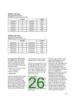
The C-Field decoder will set iERR
= 1 when it detects an error. The
internal error bit (iERR) is
combined with the internal flag
bit (iFLAG) and the flag-bit mode-
select signal (FLAGSEL) to
produce the externally available
error bit (ERROR) and flag
(FLAG) bits. If FLAGSEL=1, the
FLAG can be used as an extra
data bit:
• ERROR=iERR.
• FLAG=iFLAG.
• If a Fill Frame is detected, then
FLAG=0.
• If a Control Frame is detected,
FLAG should be ignored.
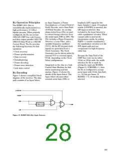
HDMP-1024 (Rx) Link-
Control State Machine
Operation Principle
The link-control state machine
(SMC) on the Rx chip provides a
link handshake protocol enabling
the duplex link to transition from
frequency acquisition and training
mode into data mode.
Considering only the local port of
the link, there is a transmitter
(Tx), a receiver (Rx) and a state
machine controller (SMC). The
SMC entity, although logically
distinct, is implemented on the
same die as the Rx chip. The SMC
monitors the data frame status
indicators (ERROR, DAV, CAV,
FW) from the Rx, and is able to
force (or control) various
characteristics of the Tx and the
Rx chips. The Tx chip has the
following controllable features:
• It can be forced to send a Fill
Frame using the ED input.
The HDMP-1022/1024 Tx/Rx link
uses an explicit frequency
acquisition mode at startup that
operates on a square-wave
training sequence. This makes it
possible to use a VCO with a very
wide tuning range yet avoid the
harmonic false lock problems
associated with other circuits of
this type.
• The type of Fill Frame sent can
be controlled using the FF
input.
If FLAGSEL=0, the serial input is
assumed to consist of alternating
even frames (iFLAG=0) and odd
frames (iFLAG=1):
• If iERR=1, then ERROR=1.
• If a Fill Frame is detected, then
FLAG=0.
• If a Data Frame is detected,
then FLAG=iFLAG, and iFLAG
should alternate between 0 and
1, starting with 0 and ending
with 1; otherwise, ERROR=1.
• If a Control Frame is detected,
then FLAG automatically
alternates between 0 and 1,
starting with 0.
The Rx Chip has the following
controllable features:
• It can be in Frequency
Using the SMC, a full duplex data
channel can be implemented
without additional controller or
hardware.
acquisition or Phase-lock/Data
reception mode depending on
the state of the FDIS input.
The State Machine
Handshake Protocol
• It can be enabled for data
reception or set in a mode in
which data frames are ignored
depending on the ACTIVE
input.
The Rx chip can also distinguish
between various types of frames.
It can also communicate the
frame type to the SMC. The
various frame types are:
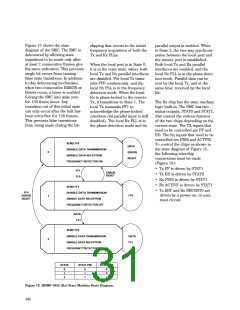
Figure 1d shows a simplified
block diagram of the HDMP-
1022/1024 data channel con-
figured for full duplex operation.
Two HDMP-1022/1024 chipsets
are required to perform the
handshake in parallel. There are
three states that the link must go
through to complete the link
startup process:
The even or odd feature allows a
32/40-bit wide data word to be
transmitted through the link. A
2:1 multiplexer and a 1:2 demulti-
plexer are required. FLAG is used
to synchronize the even and odd
frames. Note, both Data and
Control Frames can be
• Fill Frame 0, (FF0)
• Fill Frame 1 a/b (FF1)
• Data/Control frames (Data)
• Error frames (ERROR)
The SMC can also be reset by
either the SMCRST0* or
SMCRST1* inputs. Usually one of
these inputs is used for power-on
reset, and the other is connected
to the Tx LOCKED output.
• State 0: Frequency Acquisition
• State 1: Waiting for Peer
• State 2: Sending Data
Each side of the link decides
which of the three states that it
should be in. The decision is
based on its own past memory
and the type of frame that it is
currently receiving from the other
side of the link.
transmitted as even/odd pairs, but
only Data Frames can be detected
for out of order errors.
This holds the SMC in state 0 until
the transmitter PLL has locked.
645

 AGILENT [ AGILENT TECHNOLOGIES, LTD. ]