Ambassador T8100A, T8102, and T8105
H.100/H.110 Interfaces and Time-Slot Interchangers
Advance Data Sheet
November 1999
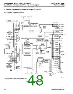
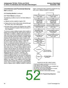
Figure 18 shows the steps required to program the reg-
isters when a fallback condition is detected.
2 Architecture and Functional Descrip-
tion (continued)
2.5 Clocking Section (continued)
2.5.7 Clock Fallback (continued)
DISABLE WATCHDOGS:
CKW = 0x00
DISABLE WATCHDOGS:
CKW = 0x00
The following conditions must be met before fallback is
initiated:
PROGRAM PRIMARY
SELECTION:
CKR, CKM, CKP,
CKMD, CKRD
REPROGRAM PRIMARY
SELECTION:
■ Fallback must be enabled in register CKS.
CKR, CKM, CKP,
CKMD, CKRD
■ Failure of one or more of the clocks selected through
the CKSEL bits in the CKM register.
PROGRAM SECONDARY
SELECTION: CKS
CLEAR FALLBACK ERROR:
MCR = 0x6E
■ All clocks which comprise the selection from CKSEL
must be unmasked in register CKW (see Section 2.7
Error Registers).
PROGRAM OTHER
CLOCKS: CKN, CKND,
CK32, CK10
REPROGRAM SECONDARY
SELECTION: CKS,
IF REQUIRED
The devices contain a fallback register which enables a
backup set of controls for the clock resources during a
clock failure. In addition, a fallback state machine pro-
vides some basic decision-making for controlling some
of the clock outputs when the feature is enabled. While
slaving to the bus, the primary course of action in fall-
back is the swap between the A clocks and B clocks as
the primary synchronization sources. A slave may
become a master only under software control; i.e.,
there is no automatic promotion mechanism. As a mas-
ter, the devices detect their own failures and remove
their clocks from the bus. If a failure is detected on the
other main set (e.g., B master detects failures on the A
master), then the devices can assume the role of the
primary synchronization source by driving all compati-
bility clocks (H-MVIP and SC-Bus). Clock failures are
flagged through the CLKERR1, CLKERR2, and
PROGRAM OTHER
REGISTERS
ENABLE WATCHDOGS:
CKW ≠ 0x00
ENABLE OUTPUTS:
MCR = 0x0E
ENABLE WATCHDOGS:
CKW ≠ 0x00
(IN
OPERATION)
FALLBACK?
YES, INTERRUPT
SERVICE ROUTINE
NO
CLKERR3 registers (Section 2.7 Error Registers).
Additional fallback details are discussed in relationship
to the clock registers in the next section. The divide-by-
4 block for XTALIN, shown in Figure 16, is used only for
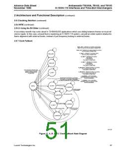
fallback. See Figure 17 for a diagram of the basic state
machine which controls the A, B, and C (compatibility)
clocks. Figure 18 shows a diagram for programming the
device’s registers when a fallback condition is detected.
RETURN FROM
INTERRUPT
CONNECT
Restarting the clocks after a fallback condition:
1. Clear the CKW register to prevent any more clock errors.
2. Clear CKM bit 5 (CCD) to be a slave.
3. Clear CKP bits 2 and 3 to prevent sourcing a compatility clock.
4. Set CKM bit 5 (CCD) to be a master again.
5. Set CKP bits 2 and 3 to drive the appropriate A or B clocks.
6. Clear SYSERR and CLKERR bits via MCR.
7. Set the appropriate bits in CKW to enable watchdogs.
5-7250aF
Figure 18. Programming Sequence
48
Lucent Technologies Inc.

 AGERE [ AGERE SYSTEMS ]