Ambassador T8100A, T8102, and T8105
H.100/H.110 Interfaces and Time-Slot Interchangers
Advance Data Sheet
November 1999
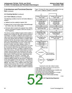
2 Architecture and Functional Description (continued)
2.5 Clocking Section (continued)
2.5.8 Clock Control Register Definitions (continued)
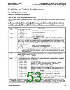
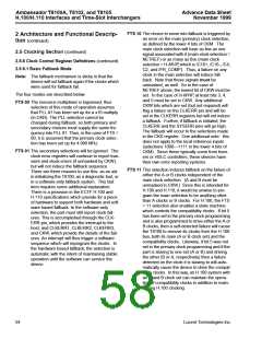
Table 49. CKR: Clocks, Resource Selection, 0x03
Clock register 0x03, CKR, is the clock resources register. It is used for selecting and programming miscellaneous
internal resources, the two PLLs, the DPLL, and the clock resource selector. It is also used to program the
SCLK/SCLKX2 clock outputs. The register format is as follows:
Reg
R/W
Bit 7
Bit 6
Bit 5
Bit 4
Bit 3
Bit 2
Bit 1
Bit 0
CKR
—
CRS
P1B
P1R
P2B
P2R
SCS
Symbol
Bit
Description
CRS
7—6 The CRS[7:6] bits are used to select the input to PLL #1.
CRS = 00,
CRS = 01,
CRS = 10,
CRS = 11,
External input (through the 4MHzIN pin).
Resource divider.
DPLL @ 2.048 MHz.
DPLL @ 4.096 MHz.
P1B
5
P1B and P1R control PLL #1.
P1B = 0,
P1B = 1,
Normal PLL #1 operation.
Bypass PLL #1.
P1R
P2B
4
3
P1R = 0,
P1R = 1,
PLL #1 rate multiplier = 16.
PLL #1 rate multiplier = 32.
P2B and P2R control PLL #2.
P2B = 0,
P2B = 1,
Normal PLL #2 operation.
Bypass PLL #2.
P2R
SCS
2
P2R = 0,
P2R = 1,
PLL #2 rate multiplier = 8.
PLL #2 rate multiplier = 16.
1—0 The SCS[1:0] bits are used to program the outgoing SC-Bus compatibility signals.
SCS = 00,
SCS = 01,
SCS = 10,
SCS = 11,
SC-Bus outputs 3-stated.
SCLK @ 2.048 MHz, SCLKX2 @ 4.096 MHz.
SCLK @ 4.096 MHz, SCLKX2 @ 8.192 MHz.
SCLK @ 8.192 MHz, SCLKX2 @ phase shifted 8.192 MHz.
52
Lucent Technologies Inc.

 AGERE [ AGERE SYSTEMS ]