Ambassador T8100A, T8102, and T8105
H.100/H.110 Interfaces and Time-Slot Interchangers
Advance Data Sheet
November 1999
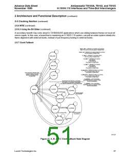
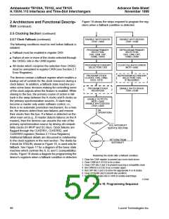
2 Architecture and Functional Description (continued)
2.5 Clocking Section (continued)
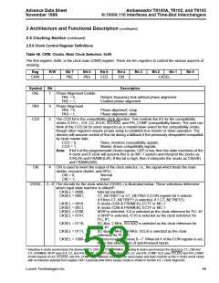
2.5.8 Clock Control Register Definitions (continued)
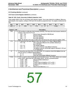
Table 47. CKN: Clocks, NETREF Selections, 0x01
Clock register 0x01 is CKN, the CT_NETREF select register. This register selects features for generating and rout-
ing the CT_NETREF signal.
Reg
R/W
Bit 7
Bit 6
Bit 5
Bit 4
Bit 3
Bit 2
Bit 1
Bit 0
CKN
—
NR12EN
NDB
NRI
NRSEL
Symbol
Bit
Description
NR12EN 7—6 NR12EN enables the selection between NETREF1 and NETREF2.
NR12EN = 00,
The value of NRSEL[3:0] of CKN determines what is routed to the
L_SCs.
NR12EN = 01,
NR12EN = 10,
NR12EN = 11,
Enable NETREF2 for output, route NETREF1 input to the L_SCs.
Enable NETREF1 for output, route NETREF2 input to the L_SCs.
Enable both NETREF[1:2] for output, route output of NETREF
divide-by-N to LSCs.
NDB
NRI
5
4
NDB = 0,
NDB = 1,
TODJAT pin comes from NETREF selector, and FROMDJAT pin
goes to NETREF divider.
NETREF selector goes directly to NETREF divider.
NRI inverts the output of the NETREF selector.
NRI = 0,
NRI = 1,
Normal.
Invert.
NRSEL 3—0 The NRSEL is similar to CKSEL but with fewer choices:
NRSEL = 0000,
NRSEL = 0001,
NRSEL = 0010,
NRSEL = 0011,
Internal oscillator divided by 8.
Internal oscillator.
Select NETREF1 as input.
Select NETREF2 as input.
NRSEL = 0100—0111, (Reserved.)
NRSEL = 1000—1111, Local references 0—7.
50
Lucent Technologies Inc.

 AGERE [ AGERE SYSTEMS ]