Ambassador T8100A, T8102, and T8105
H.100/H.110 Interfaces and Time-Slot Interchangers
Advance Data Sheet
November 1999
2 Architecture and Functional Description (continued)
2.5 Clocking Section (continued)
2.5.8 Clock Control Register Definitions
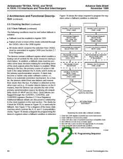
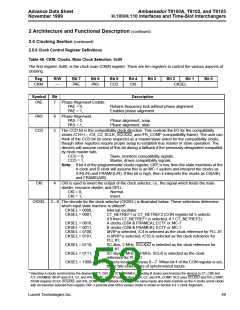
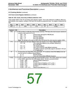
Table 46. CKM: Clocks, Main Clock Selection, 0x00
The first register, 0x00, is the clock main (CKM) register. There are ten registers to control the various aspects of
clocking.
Reg
R/W
Bit 7
Bit 6
Bit 5
Bit 4
Bit 3
Bit 2
Bit 1
Bit 0
CKM
—
PAE
PAS
CCD
CKI
CKSEL
Symbol
Bit
Description
PAE
7
6
5
Phase Alignment Enable.
PAE = 0,
Retains frequency lock without phase alignment.
Enables phase alignment.
PAE = 1,
PAS
Phase Alignment.
PAS = 0,
Phase alignment, snap.
Phase alignment, slide.
PAS = 1,
CCD
The CCD bit is the compatibility clock direction. This controls the I/O for the compatibility
clocks /C16+/–, /C4, C2, SCLK, SCLKX2, and /FR_COMP (compatibility frame). The user can
think of the CCD bit (in some respects) as a master/slave select for the compatibility clocks,
though other registers require proper setup to establish true master or slave operation. The
devices will assume control of this bit during a fallback if the previously designated compatibil-
ity clock master fails.
CCD = 0,
CCD = 1,
Slave, monitors compatibility signals.
Master, drives compatibility signals.
Note: If bit 4 of the programmable clocks register, CKP, is low, then the state machines of the
A clock and B clock will assume this is an MC-1 system and interpret the clocks as
/C4(L/R) and FRAME(L/R). If this bit is high, then it interprets the clocks as C8(A/B)
and FRAME(A/B).
CKI
4
CKI is used to invert the output of the clock selector, i.e., the signal which feeds the main
divider, resource divider, and DPLL:
CKI = 0,
CKI = 1,
Normal.
Invert.
CKSEL 3—0 The decode for the clock selector (CKSEL) is illustrated below. These selections determine
which input state machine is utilized*:
CKSEL = 0000,
CKSEL = 0001,
Internal oscillator.
CT_NETREF1 or CT_NETREF2 (CON register bit 5 selects:
if 0 then CT_NETREF1 is selected, if 1 CT_NETREF2).
A clocks (C8A & FRAMEA); ECTF or MC-1.
B clocks (C8B & FRAMEB); ECTF or MC-1.
MVIP is selected, /C4 is selected as the clock reference for PLL #1.
H-MVIP is selected, /C16 is selected as the clock reference for
PLL #1.
CKSEL = 0010,
CKSEL = 0011,
CKSEL = 0100,
CKSEL = 0101,
CKSEL = 0110,
CKSEL = 0111,
SC-Bus, 2 MHz. SCLKX2 is selected as the clock reference for
PLL #1.
SC-Bus, 4 MHz or 8 MHz. SCLK is selected as the clock
reference for PLL #1.
CKSEL = 1000—1111 Selects local references 0—7. When bit 4 of the CON register is set,
these bits select pairs of synchronized inputs.
* Selecting A clocks synchronizes the devices to CT_C8A and /CT_FRAMEA; selecting B clocks synchronizes the devices to CT_C8B and
/CT_FRAMEB; MVIP uses /C4, C2, and /FR_COMP; H-MVIP uses /C16+/–, /C4, C2, and /FR_COMP; SC2 uses SCLKX2 and /FR_COMP;
SC4/8 requires SCLK, SCLKX2, and /FR_COMP. MC-1 fallback clocks use the same inputs and state machine as the A clocks and B clocks
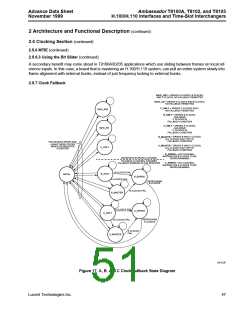
with an inversion selected from register CKP. A pictorial view of the various clocks is shown in Section 4.8.1 Clock Alignment.
Lucent Technologies Inc.
49

 AGERE [ AGERE SYSTEMS ]