Ambassador T8100A, T8102, and T8105
H.100/H.110 Interfaces and Time-Slot Interchangers
Advance Data Sheet
November 1999
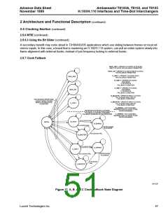
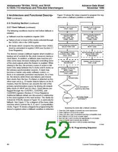
2 Architecture and Functional Description (continued)
2.5 Clocking Section (continued)
2.5.8 Clock Control Register Definitions (continued)
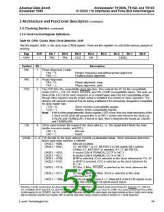
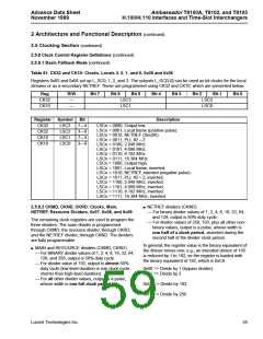
Table 48. CKP: Clocks, Programmable Outputs, 0x02
Clock register 0x02, CKP, is the programmed clocks register. It is used for programming the CT_C8 clocks and
enabling its outputs. It is also used to program the TCLK selector. CT_C8 may be operated as either 8 MHz (nor-
mal or inverted) or 4 MHz (normal or inverted). C8IS is used to invert the synchronization on C8A and C8B when
they are selected for input. The C8 and FRAME signals, which are also generated internally, are routed to both the
CT_C8A and /CT_FRAMEA and to the CT_C8B and /CT_FRAMEB. The CAE and CBE pins enable these output
pairs independently. The C8C4 pin selects 8.192 MHz or 4.096 MHz signals to be output on C8A and C8B (for sup-
porting for either ECTF or MC-1 applications). CFW selects the output width of the compatibility frame. The register
format is as follows.
Reg
R/W
Bit 7
Bit 6
Bit 5
Bit 4
Bit 3
Bit 2
Bit 1
Bit 0
CKP
—
PTS
C8IS
CAE
CBE
C8C4
CFW
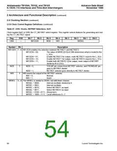
Symbol
Bit
Description
PTS
7—5 The three PTS bits select the output sent to the TCLK. This output is intended to be used for
driving framers.
PTS = 000,
PTS = 001,
PTS = 010,
PTS = 011,
PTS = 100,
PTS = 101,
PTS = 110,
PTS = 111,
3-state.
Oscillator, buffered output.
PLL #2, direct output .
PLL #2, output divided by 2.
2.048 MHz from state machines.
4.096 MHz from state machines.
8.192 MHz from state machines.
16.384 MHz from state machines.
C8IS
CAE
4
3
C8IS = 0,
C8IS = 1,
MC-1 (A and B clocks inputs interpreted as /C4 with /FRAME).
ECTF (A and B clocks inputs interpreted as C8 with /FRAME).
CAE = 0,
CAE = 1,
Disable CT_C8A & /CT_FRAMEA outputs.
Enable CT_C8A & /CT_FRAMEA outputs. (The devices will auto-
matically disable these on an A clock failure.)
CBE
2
CBE = 0,
CBE = 1,
Disable CT_C8B & /CT_FRAMEB outputs.
Enable CT_C8B & /CT_FRAMEB outputs. (The devices will auto-
matically disable these on a B clock failure.)
C8C4
CFW
1
0
C8C4 = 0,
C8C4 = 1,
Inverted 4.096 MHz (MC-1 output mode).
Noninverted 8.192 MHz (ECTF output mode).
CFW = 0,
CFW = 1,
Narrow (122 ns) /FR_COMP.
Wide (244 ns) /FR_COMP.
Lucent Technologies Inc.
51

 AGERE [ AGERE SYSTEMS ]