Ambassador T8100A, T8102, and T8105
H.100/H.110 Interfaces and Time-Slot Interchangers
Advance Data Sheet
November 1999
A digital PLL that can rate multiply to either 2.048 MHz
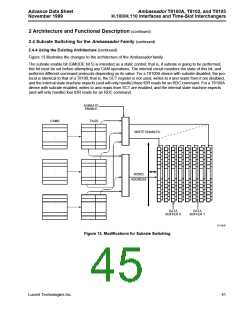
2 Architecture and Functional Descrip-
tion (continued)
or 4.096 MHz from an 8 kHz source in the absence of
an external clock adapter is also provided. PLL #1 can
be bypassed for diagnostic purposes or if an external
clock adapter is used that provides a high-speed output
(65.536 MHz). The input to the DPLL is an 8 kHz sig-
nal.
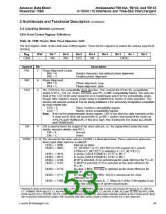
2.5 Clocking Section (continued)
2.5.1 Clock and NETREF Selection
Three selectors provide device input clocking. The
clock selector and frame selector operate from a com-
mon set of selection options in register CKM (see Sec-
tion 2.5.8 Clock Control Register Definitions for register
details), where FRAMEA is selected along with clock
C8A and FRAMEB is selected along with clock C8B.
Typically, one of the local references (L_REF[0:7]) will
be selected when the devices are operating as mas-
ters, though the local oscillator is also available. As a
slave, the most common selections will be one of the
bus types. Each bus type has a state machine associ-
ated with it for determining the frame sync. All clock
inputs are sampled to check for proper switching. If the
expected clock edge does not occur, and there is no
switching on CT_NETREF for 125 µs, a bit correspond-
ing to the errant clock is set in the CLKERR register
(see Section 2.7 Error Registers for more details).
NETREF can be created from one of the local refer-
ences or from the oscillator independent of the clock
generation.
A second rate multiplier is provided for supporting T1
applications. It is optimized around either a 1.544 MHz
or 3.088 MHz input rate which multiplies to 24.704 MHz
and is then divided down to provide 50% duty cycle
clocks of 12.352 MHz, though the direct 24.704 MHz is
available as well. A bypass is provided so that an exter-
nal clock can be buffered through the TCLK output. The
internal oscillator or the various outputs derived from
PLL #1 can also be selected for the TCLK output.
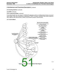
2.5.3 State Machines
The purpose of the state machines is to generate
internal control signals for the remainder of the circuitry
and to provide all bus clocks when operating as a mas-
ter. The state machines operate from the 65.536 MHz
clock generated by PLL #1, and they are time refer-
enced to the frame sync derived from the selected
clock and frame inputs. As a master, the time sync is
based on the device’s own generated frame.
The dominant internal control signals are a noninverted
32.768 MHz clock, an inverted 16.384 MHz state clock,
and a noninverted 122 ns wide sync pulse centered
around the beginning of a frame. The memories are
synchronized to the 65.536 MHz clock.
2.5.2 Dividers and Rate Multipliers
The clock and NETREF selections are routed to divid-
ers*. In the case of NETREF, the divider is
usually used to reduce a bit rate clock to 8 kHz,
so the most common divisors will be 1, 193
(1.544 MHz/8 kHz), and 256 (2.048 MHz/8 kHz),
although a full range of values (from 1—256) is possi-
ble. For the clock selector, the signal will most often be
routed through the main divider when the devices are
operating as masters or through the resource divider
when operating as slaves. Both the main and resource
dividers are fully programmable.
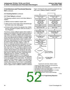
2.5.4 Frame Sync
Frame sync is not generated in absence of an external
frame clock. The state machinces will randomly syn-
chronize to the 65.536 MHz clock.
2.5.5 Bit Sliding (Frame Locking)
The devices generate frame signals based on the
incoming clock and frame references and device gen-
erated clock signals. When slaving, it is sometimes
necessary to align the edges of this generated frame
signal to the incoming frame reference.
The ultimate destination for the main or resource
divider is intended to be PLL #1. PLL #1 accepts either
a 2.048 MHz or 4.096 MHz input and will rate multiply
up to 65.536 MHz. The divisor of the main or resource
dividers is chosen in conjunction with the rate select of
the PLL, i.e., a divisor which generates a 4.096 MHz
output and a rate selection of x16, or a divisor which
generates a 2.048 MHz output and a rate selection of
x32. This provides a great deal of flexibility in adapting
to a variety of (external) clock adapters and jitter atten-
uators while acting as a master, as well as slaving to
several bus types.
* If the A clocks have been selected as the clock source through the
CKM register (described in Section 2.5.8 Clock Control Register
Definitions), then the CT_C8A is the signal sent to the main and
resource dividers; likewise, selecting B clocks results in sending
CT_C8B; the MVIP selection sends /C4; the H-MVIP selection
sends the recovered /C16 (derived from differential inputs); select-
ing SC2 sends SCLKX2; and SC4/8 sends SCLK to the dividers.
Lucent Technologies Inc.
45

 AGERE [ AGERE SYSTEMS ]