AD9834
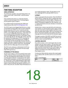
SLEEP12
SLEEP1
IOUT
SIN
ROM
0
(LOW POWER)
10-BIT DAC
PHASE
ACCUMULATOR
(28-BIT)
MUX
IOUTB
1
MSB
MODE + OPBITEN
COMPARATOR
VIN
DIVIDE
BY 2
0
MUX
1
1
DIGITAL
OUTPUT
(ENABLE)
MUX
SIGN BIT OUT
0
SIGN/PIB
OPBITEN
Figure 29. Function of Control Bits
DB15 DB14 DB13 DB12 DB11 DB10 DB9
DB8
DB7
DB6
DB5
DB4
DB3 DB2 DB1
MODE
DB0
0
0
B28 HLB FSEL PSEL PIN/SW RESET SLEEP1 SLEEP12 OPBITEN SIGN/PIB DIV2
0
0
Table 6. Description of Bits in the Control Register
Bit
Name
Description
DB13 B28
Two write operations are required to load a complete word into either of the frequency registers.
B28 = 1 allows a complete word to be loaded into a frequency register in two consecutive writes. The first write
contains the 14 LSBs of the frequency word and the next write contains the 14 MSBs. The first two bits of each 16-bit
word define the frequency register the word is loaded to and should, therefore, be the same for both of the
consecutive writes. Refer to Table 10 for the appropriate addresses. The write to the frequency register occurs after both
words have been loaded. An example of a complete 28-bit write is shown in Table 11. Note however, that consecutive
28-bit writes to the same frequency register are not allowed, switch between frequency registers to do this type of
function.
B28 = 0, the 28-bit frequency register operates as two 14-bit registers, one containing the 14 MSBs and the other
containing the 14 LSBs. This means that the 14 MSBs of the frequency word can be altered independent of the 14 LSBs,
and vice versa. To alter the 14 MSBs or the 14 LSBs, a single write is made to the appropriate frequency address. The
Control Bit DB12 (HLB) informs the AD9834 whether the bits to be altered are the 14 MSBs or 14 LSBs.
DB12 HLB
This control bit allows the user to continuously load the MSBs or LSBs of a frequency register ignoring the remaining
14 bits. This is useful if the complete 28-bit resolution is not required. HLB is used in conjunction with DB13 (B28). This
control bit indicates whether the 14 bits being loaded are being transferred to the 14 MSBs or 14 LSBs of the addressed
frequency register. DB13 (B28) must be set to 0 to be able to change the MSBs and LSBs of a frequency word separately.
When DB13 (B28) = 1, this control bit is ignored.
HLB = 1 allows a write to the 14 MSBs of the addressed frequency register.
HLB = 0 allows a write to the 14 LSBs of the addressed frequency register.
DB11 FSEL
DB10 PSEL
The FSEL bit defines whether the FREQ0 register or the FREQ1 register is used in the phase accumulator. See Table 8 to
select a frequency register.
The PSEL bit defines whether the PHASE0 register data or the PHASE1 register data is added to the output of the phase
accumulator. See Table 9 to select a phase register.
DB9
PIN/SW
Functions that select frequency and phase registers, reset internal registers, and power down the DAC can be
implemented using either software or hardware. PIN/SW selects the source of control for these functions.
PIN/SW = 1 implies that the functions are being controlled using the appropriate control pins.
PIN/SW = 0 implies that the functions are being controlled using the appropriate control bits.
RESET = 1 resets internal registers to 0, this corresponds to an analog output of midscale.
RESET = 0 disables RESET. This function is explained in the RESET Function section.
SLEEP1 = 1, the internal MCLK is disabled. The DAC output remains at its present value as the NCO is no longer
accumulating.
DB8
DB7
RESET
SLEEP1
SLEEP1 = 0, MCLK is enabled. This function is explained in the SLEEP Function section.
DB6
SLEEP12
SLEEP12 = 1 powers down the on-chip DAC. This is useful when the AD9834 is used to output the MSB of the DAC data.
SLEEP12 = 0 implies that the DAC is active. This function is explained in the SLEEP Function section.
Rev. C | Page 19 of 36

 ADI [ ADI ]