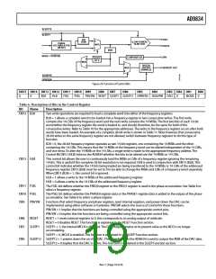
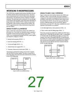
AD9834
APPLICATIONS INFORMATION
pin, causing the AD9834 to modulate the carrier frequency
between the two values.
Because of the various output options available from the part,
the AD9834 can be configured to suit a wide variety of
applications.
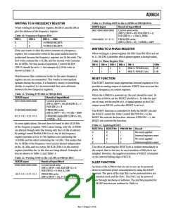
The AD9834 has two phase registers, enabling the part to
perform PSK. With phase shift keying, the carrier frequency is
phase shifted, the phase being altered by an amount that is
related to the bit stream that is input to the modulator.
One of the areas where the AD9834 is suitable is in modulation
applications. The part can be used to perform simple modulation
such as FSK. More complex modulation schemes such as GMSK
and QPSK can also be implemented using the AD9834.
The AD9834 is also suitable for signal generator applications.
With the on-board comparator, the device can be used to
generate a square wave.
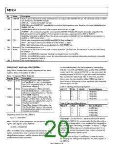
In an FSK application, the two frequency registers of the
AD9834 are loaded with different values. One frequency
represents the space frequency, and the other represents the
mark frequency. The digital data stream is fed to the FSELECT
With its low current consumption, the part is suitable for
applications where it is used as a local oscillator.
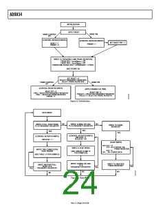
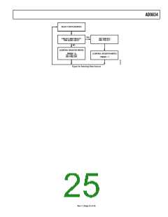
DATA WRITE
SEE FIGURE 33
SELECT DATA
SOURCES
SEE FIGURE 34
WAIT 8/9 MCLK
CYCLES
SEE TIMING DIAGRAM
FIGURE 3
INITIALIZATION
SEE FIGURE 32
DAC OUTPUT
× (1 + (SIN(2π(FREQREG × f
28 12
× t/2 + PHASEREG/2 ))))
MCLK
V
= V
× 18 × R
/R
OUT
REFOUT
LOAD SET
YES
YES
CHANGE PSEL/
PSELECT?
CHANGE PHASE?
NO
NO
YES
YES
YES
CHANGE PHASE
REGISTER?
CHANGE FSEL/
FSELECT?
CHANGE FREQUENCY?
NO
YES
NO
CHANGE DAC OUTPUT
FROM SIN TO RAMP?
CHANGE FREQUENCY
REGISTER?
YES
YES
NO
CHANGE OUTPUT AT
SIGN BIT OUT PIN?
CONTROL
REGISTER
WRITE
NO
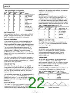
Figure 31. Flow Chart for Initialization and Operation
Rev. C | Page 23 of 36

 ADI [ ADI ]