AD9834
CIRCUIT DESCRIPTION
The AD9834 is a fully integrated direct digital synthesis (DDS)
chip. The chip requires one reference clock, one low precision
resistor, and eight decoupling capacitors to provide digitally created
sine waves up to 37.5 MHz. In addition to the generation of this RF
signal, the chip is fully capable of a broad range of simple and
complex modulation schemes. These modulation schemes are
fully implemented in the digital domain, allowing accurate and
simple realization of complex modulation algorithms using DSP
techniques.
SIN ROM
To make the output from the NCO useful, it must be converted
from phase information into a sinusoidal value. Phase informa-
tion maps directly into amplitude; therefore, the SIN ROM uses
the digital phase information as an address to a look-up table
and converts the phase information into amplitude.
Although the NCO contains a 28-bit phase accumulator, the
output of the NCO is truncated to 12 bits. Using the full resolu-
tion of the phase accumulator is impractical and unnecessary
because it requires a look-up table of 228 entries. It is necessary
only to have sufficient phase resolution such that the errors due
to truncation are smaller than the resolution of the 10-bit DAC.
This requires the SIN ROM to have two bits of phase resolution
more than the 10-bit DAC.
The internal circuitry of the AD9834 consists of the following
main sections: a numerically controlled oscillator (NCO),
frequency and phase modulators, SIN ROM, a DAC, a
comparator, and a regulator.
NUMERICALLY CONTROLLED OSCILLATOR PLUS
PHASE MODULATOR
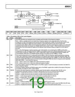
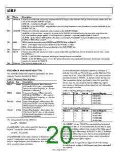
The SIN ROM is enabled using the OPBITEN and MODE bits
in the control register. This is explained further in Table 18.
This consists of two frequency select registers, a phase accumulator,
two phase offset registers, and a phase offset adder. The main
component of the NCO is a 28-bit phase accumulator. Continuous
time signals have a phase range of 0 π to 2π. Outside this range of
numbers, the sinusoid functions repeat themselves in a periodic
manner. The digital implementation is no different. The
accumulator simply scales the range of phase numbers into a
multibit digital word. The phase accumulator in the AD9834 is
implemented with 28 bits. Therefore, in the AD9834, 2π = 228.
Likewise, the ΔPhase term is scaled into this range of numbers:
DIGITAL-TO-ANALOG CONVERTER (DAC)
The AD9834 includes a high impedance current source 10-bit
DAC capable of driving a wide range of loads. The full-scale
output current can be adjusted for optimum power and external
load requirements using a single external resistor (RSET).
The DAC can be configured for either single-ended or differential
operation. IOUT and IOUTB can be connected through equal
external resistors to AGND to develop complementary output
voltages. The load resistors can be any value required, as long as
the full-scale voltage developed across it does not exceed the
voltage compliance range. Because full-scale current is
controlled by RSET, adjustments to RSET can balance changes
made to the load resistors.
0 < ΔPhase < 228 − 1.
Making these substitutions into the previous equation
f = ΔPhase × fMCLK/228
where 0 < ΔPhase < 228 − 1.
COMPARATOR
The input to the phase accumulator can be selected either from
the FREQ0 register or FREQ1 register and is controlled by the
FSELECT pin or the FSEL bit. NCOs inherently generate con-
tinuous phase signals, thus avoiding any output discontinuity
when switching between frequencies.
The AD9834 can be used to generate synthesized digital clock
signals. This is accomplished by using the on-board self-biasing
comparator that converts the sinusoidal signal of the DAC to a
square wave. The output from the DAC can be filtered externally
before being applied to the comparator input. The comparator
reference voltage is the time average of the signal applied to VIN.
The comparator can accept signals in the range of approximately
100 mV p-p to 1 V p-p. As the comparator input is ac-coupled, to
operate correctly as a zero crossing detector, it requires a minimum
input frequency of typically 3 MHz. The comparator output is a
square wave with an amplitude from 0 V to DVDD.
Following the NCO, a phase offset can be added to perform
phase modulation using the 12-bit phase registers. The contents
of one of these phase registers is added to the MSBs of the NCO.
The AD9834 has two phase registers, the resolution of these
registers being 2π/4096.
Rev. C | Page 16 of 36

 ADI [ ADI ]