AD9834
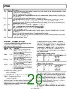
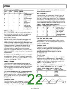
Table 16. Applying the SLEEP Function
from the DAC, the waveform can be applied to the comparator
to generate a square waveform.
SLEEP
Pin
SLEEP1 SLEEP12 PIN/SW
Bit
Bit
Bit
Result
MSB from the NCO
0
1
X
X
X
X
1
1
No power-down
DAC powered
down
No power-down
DAC powered
down
The MSB from the NCO can be output from the AD9834. By
setting the SIGN/PIB (DB4) control bit to 0, the MSB of the
DAC data is available at the SIGN BIT OUT pin. This is useful
as a coarse clock source. This square wave can also be divided
by two before being output. Bit DIV2 (DB3) in the control register
controls the frequency of this output from the SIGN BIT OUT pin.
X
X
0
0
0
1
0
0
X
X
1
1
0
1
0
0
Internal clocꢀ
disabled
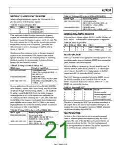
Table 17. Various Outputs from SIGN BIT OUT
Both the DAC
powered down
and the internal
clocꢀ disabled
OPBITEN MODE SIGN/PIB DIV2
Bit
Bit
X
0
Bit
Bit
SIGN BIT OUT Pin
High impedance
DAC data MSB/2
DAC data MSB
Reserved
0
1
X
0
X
0
DAC Powered Down
1
0
0
1
This is useful when the AD9834 is used to output the MSB of
the DAC data only. In this case, the DAC is not required and
can be powered down to reduce power consumption.
1
0
1
0
1
1
0
1
1
X
1
X
Comparator output
Reserved
Internal Clock Disabled
THE IOUT AND IOUTB PINS
When the internal clock of the AD9834 is disabled, the DAC
output remains at its present value because the NCO is no
longer accumulating. New frequency, phase, and control words
can be written to the part when the SLEEP1 control bit is active.
The synchronizing clock remains active, meaning that the
selected frequency and phase registers can also be changed
either at the pins or by using the control bits. Setting the
SLEEP1 bit to 0 enables the MCLK. Any changes made to the
registers when SLEEP1 is active are observed at the output after
a certain latency.
The analog outputs from the AD9834 are available from the
IOUT and IOUTB pins. The available outputs are a sinusoidal
output or a triangle output.
Sinusoidal Output
The SIN ROM converts the phase information from the
frequency and phase registers into amplitude information,
resulting in a sinusoidal signal at the output. To have a
sinusoidal output from the IOUT and IOUTB pins, set
Bit MODE (DB1) to 0.
The effect of asserting the SLEEP pin is evident immediately at
the output, that is, the zero-to-one transition of this pin is not
sampled. However, the negative transition of SLEEP is sampled
on the internal falling edge of MCLK.
Triangle Output
The SIN ROM can be bypassed so that the truncated digital
output from the NCO is sent to the DAC. In this case, the
output is no longer sinusoidal. The DAC produces 10-bit linear
triangular function. To have a triangle output from the IOUT
and IOUTB pins, set Bit MODE (DB1) to 1.
SIGN BIT OUT PIN
The AD9834 offers a variety of outputs from the chip. The
digital outputs are available from the SIGN BIT OUT pin. The
available outputs are the comparator output or the MSB of the
DAC data. The bits controlling the SIGN BIT OUT pin are
outlined in Table 17.
Note that the SLEEP pin and SLEEP12 bit must be 0 (that is, the
DAC is enabled) when using the IOUT and IOUTB pins.
Table 18. Various Outputs from IOUT and IOUTB
OPBITEN Bit
MODE Bit
IOUT and IOUTB Pins
0
0
1
1
0
1
0
1
Sinusoid
Triangle
Sinusoid
Reserved
This pin must be enabled before use. The enabling/disabling of
this pin is controlled by the Bit OPBITEN (DB5) in the control
register. When OPBITEN = 1, this pin is enabled. Note that the
MODE bit (DB1) in the control register should be set to 0 if
OPBITEN = 1.
V
OUT MAX
Comparator Output
V
The AD9834 has an on-board comparator. To connect this
comparator to the SIGN BIT OUT pin, the SIGN/PIB (DB4)
control bit must be set to 1. After filtering the sinusoidal output
OUT MIN
3π/2
7π/2
11π/2
Figure 30. Triangle Output
Rev. C | Page 22 of 36

 ADI [ ADI ]