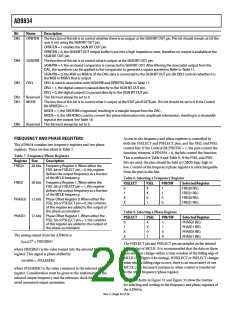
AD9834
Bit
Name
Description
DB5
OPBITEN The function of this bit is to control whether there is an output at the SIGN BIT OUT pin. This bit should remain at 0 if the
user is not using the SIGN BIT OUT pin.
OPBITEN = 1 enables the SIGN BIT OUT pin.
OPBITEN = 0, the SIGN BIT OUT output buffer is put into a high impedance state, therefore no output is available at the
SIGN BIT OUT pin.
DB4
DB3
SIGN/PIB The function of this bit is to control what is output at the SIGN BIT OUT pin.
SIGN/PIB = 1, the on-board comparator is connected to SIGN BIT OUT. After filtering the sinusoidal output from the
DAC, the waveform can be applied to the comparator to generate a square waveform. Refer to Table 17.
SIGN/PIB = 0, the MSB (or MSB/2) of the DAC data is connected to the SIGN BIT OUT pin. Bit DIV2 controls whether it is
the MSB or MSB/2 that is output.
DIV2
DIV2 is used in association with SIGN/PIB and OPBITEN. Refer to Table 17.
DIV2 = 1, the digital output is passed directly to the SIGN BIT OUT pin.
DIV2 = 0, the digital output/2 is passed directly to the SIGN BIT OUT pin.
DB2
DB1
Reserved This bit must always be set to 0.
MODE
The function of this bit is to control what is output at the IOUT pin/IOUTB pin. This bit should be set to 0 if the Control
Bit OPBITEN = 1.
MODE = 1, the SIN ROM is bypassed, resulting in a triangle output from the DAC.
MODE = 0, the SIN ROM is used to convert the phase information into amplitude information, resulting in a sinusoidal
signal at the output. See Table 18.
DB0
Reserved This bit must always be set to 0.
Access to the frequency and phase registers is controlled by
both the FSELECT and PSELECT pins, and the FSEL and PSEL
control bits. If the Control Bit PIN/SW = 1, the pins control the
function; whereas, if PIN/SW = 0, the bits control the function.
This is outlined in Table 8 and Table 9. If the FSEL and PSEL
bits are used, the pins should be held at CMOS logic high or
low. Control of the frequency/phase registers is interchangeable
from the pins to the bits.
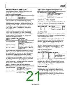
FREQUENCY AND PHASE REGISTERS
The AD9834 contains two frequency registers and two phase
registers. These are described in Table 7.
Table 7. Frequency/Phase Registers
Register Size
Description
FREQ0
28 bits Frequency Register 0. When either the
FSEL bit or FSELECT pin = 0, this register
defines the output frequency as a fraction
of the MCLK frequency.
Table 8. Selecting a Frequency Register
FREQ1
28 bits Frequency Register 1. When either the
FSEL bit or FSELECT pin = 1, this register
defines the output frequency as a fraction
of the MCLK frequency.
FSELECT
FSEL
PIN/SW
Selected Register
0
1
X
X
X
X
0
1
1
1
0
0
FREQ0 REG
FREQ1 REG
FREQ0 REG
FREQ1 REG
PHASE0
PHASE1
12 bits Phase Offset Register 0. When either the
PSEL bit or PSELECT pin = 0, the contents
of this register are added to the output of
the phase accumulator.
12 bits Phase Offset Register 1. When either the
PSEL bit or PSELECT pin = 1, the contents
of this register are added to the output of
the phase accumulator.
Table 9. Selecting a Phase Register
PSELECT
PSEL
PIN/SW
Selected Register
PHASE0 REG
PHASE1 REG
PHASE0 REG
PHASE1 REG
0
1
X
X
X
X
0
1
1
1
0
0
The analog output from the AD9834 is
fMCLK/228 × FREQREG
The FSELECT pin and PSELECT pin are sampled on the internal
falling edge of MCLK. It is recommended that the data on these
pins does not change within a time window of the falling edge of
MCLK (see Figure 4 for timing). If FSELECT or PSELECT changes
value when a falling edge occurs, there is an uncertainty of one
MCLK cycle because it pertains to when control is transferred
to the other frequency/phase register.
where FREQREG is the value loaded into the selected frequency
register. This signal is phase shifted by
2π/4096 × PHASEREG
where PHASEREG is the value contained in the selected phase
register. Consideration must be given to the relationship of the
selected output frequency and the reference clock frequency to
avoid unwanted output anomalies.
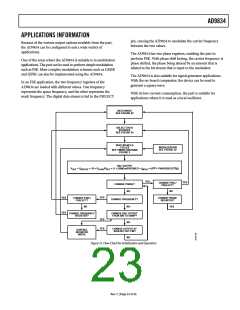
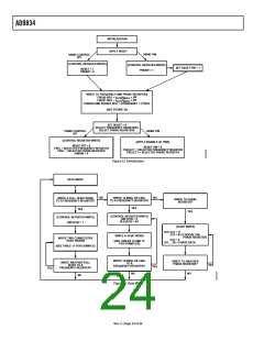
The flow charts in Figure 32 and Figure 33 show the routine
for selecting and writing to the frequency and phase registers of
the AD9834.
Rev. C | Page 20 of 36

 ADI [ ADI ]