AD9834
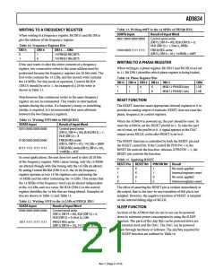
Table 13. Writing 00FF to the 14 MSBs of FREQ0 REG
WRITING TO A FREQUENCY REGISTER
SDATA Input
Result of Input Word
When writing to a frequency register, Bit DB15 and Bit DB14
give the address of the frequency register.
0001 0000 0000 0000
Control word write
(DB15, DB14 = 00), B28 (DB13) = 0,
HLB (DB12) = 1, that is, MSBs
Table 10. Frequency Register Bits
DB15
DB14
DB13 . . . DB0
0100 0000 1111 1111
FREQ0 REG write
(DB15, DB14 = 01), 14 MSBs = 00FF
0
1
1
0
14 FREQ0 REG BITS
14 FREQ1 REG BITS
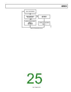
WRITING TO A PHASE REGISTER
If the user wants to alter the entire contents of a frequency
register, two consecutive writes to the same address must be
performed because the frequency registers are 28 bits wide. The
first write contains the 14 LSBs, and the second write contains
the 14 MSBs. For this mode of operation, Control Bit B28
(DB13) should be set to 1. An example of a 28-bit write is
shown in Table 11.
When writing to a phase register, Bit DB15 and Bit DB14 are set
to 11. Bit DB13 identifies which phase register is being loaded.
Table 14. Phase Register Bits
DB15 DB14 DB13 DB12 DB11
DB0
LSB
LSB
1
1
1
1
0
1
X
X
MSB 12 PHASE0 bits
MSB 12 PHASE1 bits
Note however that continuous writes to the same frequency
register are not recommended. This results in intermediate
updates during the writes. If a frequency sweep, or something
similar, is required, it is recommended that users alternate
between the two frequency registers.
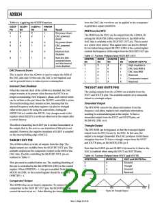
RESET FUNCTION
The RESET function resets appropriate internal registers to 0 to
provide an analog output of midscale. RESET does not reset the
phase, frequency, or control registers.
Table 11. Writing FFFC000 to FREQ0 REG
When the AD9834 is powered up, the part should be reset. To
reset the AD9834, set the RESET pin/bit to 1. To take the part
out of reset, set the pin/bit to 0. A signal appears at the DAC
output seven MCLK cycles after RESET is set to 0.
SDATA Input
Result of Input Word
0010 0000 0000 0000
Control word write
(DB15, DB14 = 00), B28 (DB13) = 1,
HLB (DB12) = X
0100 0000 0000 0000
0111 1111 1111 1111
FREQ0 REG write
(DB15, DB14 = 01), 14 LSBs = 0000
FREQ0 REG write (DB15, DB14 = 01),
14 MSBs = 3FFF
The RESET function is controlled by both the RESET pin and
the RESET control bit. If the Control Bit PIN/SW = 0, the
RESET bit controls the function, whereas if PIN/SW = 1, the
RESET pin controls the function.
In some applications, the user does not need to alter all 28 bits
of the frequency register. With coarse tuning, only the 14 MSBs
are altered; though with fine tuning only the 14 LSBs are altered.
By setting Control Bit B28 (DB13) to 0, the 28-bit frequency
register operates as two 14-bit registers, one containing the
14 MSBs and the other containing the 14 LSBs. This means that
the 14 MSBs of the frequency word can be altered independent
of the 14 LSBs, and vice versa. Bit HLB (DB12) in the control
register identifies the 14 bits that are being altered. Examples of
this are shown in Table 12 and Table 13.
Table 15. Applying RESET
RESET Pin RESET Bit PIN/SW Bit Result
0
1
X
X
X
X
0
1
1
1
0
0
No reset applied
Internal registers reset
No reset applied
Internal registers reset
The effect of asserting the RESET pin is evident immediately at
the output, that is, the zero-to-one transition of this pin is not
sampled. However, the negative transition of RESET is sampled
on the internal falling edge of MCLK.
Table 12. Writing 3FFF to the 14 LSBs of FREQ1 REG
SDATA Input
Result of Input Word
SLEEP FUNCTION
0000 0000 0000 0000
Control word write
Sections of the AD9834 that are not in use can be powered
down to minimize power consumption by using the SLEEP
function. The parts of the chip that can be powered down are
the internal clock and the DAC. The DAC can be powered
down through hardware or software. The pin/bits required for
the SLEEP function are outlined in Table 16.
(DB15, DB14 = 00), B28 (DB13) = 0,
HLB (DB12) = 0, that is, LSBs
FREQ1 REG write
1011 1111 1111 1111
(DB15, DB14 = 10), 14 LSBs = 3FFF
Rev. C | Page 21 of 36

 ADI [ ADI ]