AD9834
FUNCTIONAL DESCRIPTION
to 0 to begin generating an output. The data appears on the
DAC output eight MCLK cycles after RESET is set to 0.
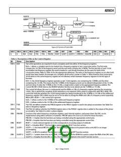
SERIAL INTERFACE
The AD9834 has a standard 3-wire serial interface that is com-
patible with SPI, QSPI™, MICROWIRE™, and DSP interface
standards.
LATENCY
Latency is associated with each operation. When Pin FSELECT
and Pin PSELECT change value, there is a pipeline delay before
control is transferred to the selected register. When the t11 and
t11A timing specifications are met (see Figure 4), FSELECT and
PSELECT have latencies of eight MCLK cycles. When the t11 and
t11A timing specifications are not met, the latency is increased by
one MCLK cycle.
Data is loaded into the device as a 16-bit word under the
control of a serial clock input (SCLK). The timing diagram
for this operation is given in Figure 5.
For a detailed example of programming the AD9833 and
AD9834 devices, refer to the AN-1070 Application Note.
The FSYNC input is a level triggered input that acts as a frame
synchronization and chip enable. Data can only be transferred
into the device when FSYNC is low. To start the serial data
transfer, FSYNC should be taken low, observing the minimum
FSYNC-to-SCLK falling edge setup time (t7). After FSYNC goes
low, serial data is shifted into the input shift register of the
device on the falling edges of SCLK for 16 clock pulses. FSYNC
can be taken high after the 16th falling edge of SCLK, observing
the minimum SCLK falling edge to FSYNC rising edge time
(t8). Alternatively, FSYNC can be kept low for a multiple of
16 SCLK pulses and then brought high at the end of the data
transfer. In this way, a continuous stream of 16-bit words can be
loaded while FSYNC is held low, with FSYNC only going high
after the 16th SCLK falling edge of the last word is loaded.
Similarly, there is a latency associated with each asynchronous
write operation. If a selected frequency/phase register is loaded
with a new word, there is a delay of eight to nine MCLK cycles
before the analog output changes. There is an uncertainty of one
MCLK cycle because it depends on the position of the MCLK
rising edge when the data is loaded into the destination register.
The negative transition of the RESET and SLEEP functions are
sampled on the internal falling edge of MCLK. Therefore, they
also have a latency associated with them.
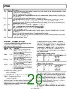
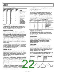
CONTROL REGISTER
The AD9834 contains a 16-bit control register that sets up the
AD9834 as the user wants to operate it. All control bits, except
MODE, are sampled on the internal negative edge of MCLK.
Table 6 describes the individual bits of the control register. The
different functions and the various output options from the
AD9834 are described in more detail in the Frequency and
Phase Registers section.
The SCLK can be continuous, or alternatively, the SCLK can
idle high or low between write operations but must be high
when FSYNC goes low (t12).
POWERING UP THE AD9834
To inform the AD9834 that the contents of the control register
are to be altered, DB15 and DB14 must be set to 0 as shown in
Table 5.
The flow chart in Figure 31 shows the operating routine for the
AD9834. When the AD9834 is powered up, the part should be
reset. This resets appropriate internal registers to 0 to provide
an analog output of midscale. To avoid spurious DAC outputs
during AD9834 initialization, the RESET bit/pin should be set
to 1 until the part is ready to begin generating an output. RESET
does not reset the phase, frequency, or control registers. These
registers contain invalid data, and, therefore, should be set to a
known value by the user. The RESET bit/pin should then be set
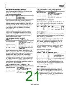
Table 5. Control Register
DB15
DB14
DB13 . . . DB0
0
0
CONTROL bits
Rev. C | Page 18 of 36

 ADI [ ADI ]