AD5940
Data Sheet
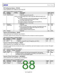
FIFO Configuration Register—FIFOCON
Address 0x00002008, Reset: 0x00001010, Name: FIFOCON
Table 95. Bit Descriptions for FIFOCON Register
Bits
Bit Name
Settings
Description
Reset Access
[31:16] RESERVED
[15:13] DATAFIFOSRCSEL
Reserved.
Selects the source for the data FIFO.
0x0
0x0
R
R/W
000, 001, 110, ADC data. ADC data is output of gain/offset calibration through the sinc3
or 111 filter.
010 DFT data. Real part is 18 bits and the imaginary part is 18 bits. The lowest
two bits are fractional because the ADC is 16 bits.
011 Sinc2 filter output. Data is 16 bits.
100 Variance. Variance is 30-bit data, which uses two addresses.
101 Mean result. Mean is 16 bits of data.
Reserved.
12
11
Reserved
DATAFIFOEN
0x1
0x0
R/W
R/W
Data FIFO enable.
0
1
FIFO is reset. No data transfers can take place. This setting sets the read
and write pointers to the default values (empty FIFO). The status
indicates that the FIFO is empty.
Normal operation. The FIFO is not reset.
Reserved.
[10:0]
Reserved
0x0
R/W
Sequencer CRC Value Register—SEQCRC
Address 0x00002060, Reset: 0x00000001, Name: SEQCRC
The SEQCRC register forms the checksum value calculated from all the commands executed by the sequencer.
Table 96. Bit Descriptions for SEQCRC Register
Bits
[31:8]
[7:0]
Bit Name
Reserved
CRC
Settings
Description
Reserved.
Reset
0x0
0x1
Access
R
R
Sequencer command CRC value. The algorithm used is CRC-8.
Sequencer Command Count Register—SEQCNT
Address 0x00002064, Reset: 0x00000000, Name: SEQCNT
The SEQCNT register forms the command count, which is incremented by 1 each time the sequencer executes a command. This register
is not key protected.
Table 97. Bit Descriptions for SEQCNT Register
Bits
[31:16] Reserved
[15:0] Count
Bit Name
Settings Description
Reset Access
Reserved.
0x0
0x0
R
Sequencer command count. This count is incremented by 1 each time the
R/W1
sequencer executes a command. Reset to 0 by writing 1 to this register. Write 1 to
this register also to clear the SEQCRC register.
Sequencer Timeout Counter Register—SEQTIMEOUT
Address 0x00002068, Reset: 0x00000000, Name: SEQTIMEOUT
Table 98. Bit Descriptions for SEQTIMEOUT Register
Bits
[31:30]
[29:0]
Bit Name
Reserved
Timeout
Settings
Description
Reserved.
Current value of the sequencer timeout counter.
Reset
0x0
0x0
Access
R
R
Rev. 0 | Page 88 of 130

 ADI [ ADI ]