Data Sheet
AD5940
SEQUENCER AND FIFO REGISTERS
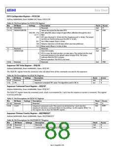
Table 93. Sequence and FIFO Registers Summary
Address
Name
Description
Reset
Access
R/W
R/W
R
R/W
R
0x00002004
0x00002008
0x00002060
0x00002064
0x00002068
0x0000206C
0x00002070
0x00002118
0x0000211C
0x000021CC
0x000021D0
0x000021D4
0x000021D8
0x000021E0
0x000021E4
0x000021E8
0x00002200
0x00002054
0x00000430
SEQCON
FIFOCON
SEQCRC
SEQCNT
SEQTIMEOUT
DATAFIFORD
CMDFIFOWRITE
SEQSLPLOCK
SEQTRGSLP
SEQ0INFO
Sequencer configuration register
FIFO configuration register
Sequencer CRC value register
Sequencer command count register
Sequencer timeout counter register
Data FIFO read register
Command FIFO write register
Sequencer sleep control lock register
Sequencer trigger sleep register
Sequence 0 information register
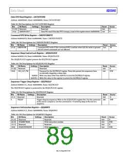
Sequence 2 information register
Command FIFO write address register
Command data control register
Data FIFO threshold register
Sequence 3 information register
Sequence 1 information register
Command and data FIFO internal data count register
Sync external devices register
Trigger sequence register
0x00000002
0x00001010
0x00000001
0x00000000
0x00000000
0x00000000
0x00000000
0x00000000
0x00000000
0x00000000
0x00000000
0x00000000
0x00000410
0x00000000
0x00000000
0x00000000
0x00000000
0x00000000
0x0000
R
W
R/W
R/W
R/W
R/W
R/W
R/W
R/W
R/W
R/W
R
SEQ2INFO
CMDFIFOWADDR
CMDDATACON
DATAFIFOTHRES
SEQ3INFO
SEQ1INFO
FIFOCNTSTA
SYNCEXTDEVICE
TRIGSEQ
R/W
R/WS
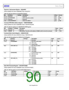
Sequencer Configuration Register—SEQCON
Address 0x00002004, Reset: 0x00000002, Name: SEQCON
Table 94. Bit Descriptions for SEQCON Register
Bits
Bit Name
Settings Description
Reset Access
[31:16] Reserved
Reserved.
0x0
0x0
R
[15:8]
SEQWRTMR
Timer for sequencer write commands. These bits act as a clock divider
R/W
affecting the write commands, but not the wait commands. This divider is
useful to reduce the code size when generating arbitrary waveforms. The
clock source for the timer is ACLK.
[7:5]
4
Reserved
SEQHALT
Reserved.
0x0
0x0
R
R/W
Halt sequence debugging feature. This bit provides a way to halt the AFE
interface, including the sequencer, DSP hardware accelerators, FIFOs, and
so on.
0
1
Normal execution.
Execution halted.
Reserved
[3:2]
1
Reserved
0x0
0x1
R
SEQHALTFIFOEMPTY
Halt sequencer, if empty. This bit controls whether the sequencer stops
when attempting to read when the command FIFO is empty (in an
underflow condition).
R/W
1
0
Sequencer stops if command FIFO is empty and sequencer attempts to
read (in an underflow condition).
Sequencer continues to attempt to read, even if the FIFO is empty.
0
SEQEN
Enable sequencer. If this bit is set to 1, the sequencer reads from the
command FIFO and executes the commands.
0x0
R/W
0
1
Sequencer disabled (default).
Sequencer enabled.
Rev. 0 | Page 87 of 130

 ADI [ ADI ]