ADSP-BF542/ADSP-BF544/ADSP-BF547/ADSP-BF548/ADSP-BF549
DDR SDRAM/Mobile DDR SDRAM Write Cycle Timing
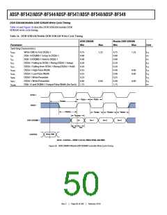
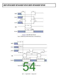
Table 34 and Figure 20 describe DDR SDRAM/mobile DDR
SDRAM write cycle timing.
Table 34. DDR SDRAM/Mobile DDR SDRAM Write Cycle Timing
DDR SDRAM
Min
Mobile DDR SDRAM
Parameter
Max
Min
Max
Unit
Switching Characteristics
tDQSS
tDS
Write CMD to First DQS0-1
0.75
0.90
0.90
0.20
0.20
0.35
0.35
0.25
0.40
1.25
0.75
0.90
0.90
0.20
0.20
0.40
0.40
0.25
0.40
1.75
1.25
tCK
ns
ns
tCK
tCK
tCK
tCK
tCK
tCK
ns
DQ0-15/DQM0-1 Setup to DQS0-1
DQ0-15/DQM0-1 Hold to DQS0-1
DQS0-1 Falling to DCK0-1 Rising (DQS0-1 Setup)
DQS0-1 Falling from DCK0-1 Rising (DQS0-1 Hold)
DQS0-1 High Pulse Width
tDH
tDSS
tDSH
tDQSH
tDQSL
tWPRE
tWPST
tDOPW
0.60
0.60
DQS0-1 Low Pulse Width
DQS0-1 Write Preamble
DQS0-1 Write Postamble
0.60
0.60
DQ0-15 and DQM0-1 Output Pulse Width (for Each) 1.75
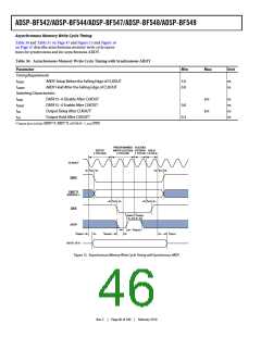
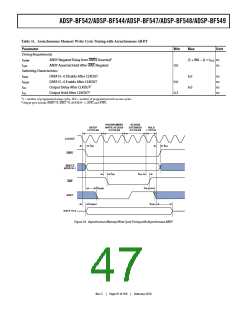
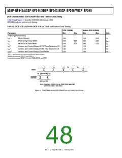
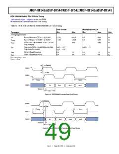
DCK0-1
t
t
DSS
DSH
t
DQSS
DQS0-1
t
WPRE
t
t
t
WPST
DQSL
DQSH
t
DOPW
Dn
DQ0-15/DQM0-1
CONTROL
Dn+1
Dn+2
Dn+3
t
t
DH
DS
Write CMD
NOTE: CONTROL = DCS0-1, DCLKE, DRAS, DCAS, AND DWE.
Figure 20. DDR SDRAM /Mobile DDR SDRAM Controller Write Cycle Timing
Rev. C
|
Page 50 of 100
|
February 2010

 ADI [ ADI ]