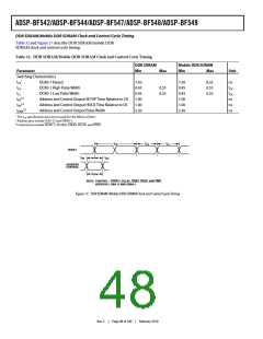
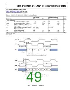
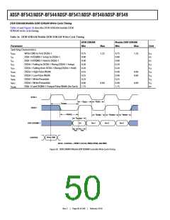
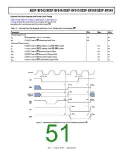
ADSP-BF542/ADSP-BF544/ADSP-BF547/ADSP-BF548/ADSP-BF549
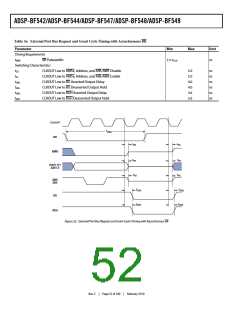
Table 36. External Port Bus Request and Grant Cycle Timing with Asynchronous BR
Parameter
Min
Max
Unit
Timing Requirements
tWBR
BR Pulsewidth
2 x tSCLK
ns
Switching Characteristics
tSD
CLKOUT Low to AMSx, Address, and ARE/AWE Disable
5.0
5.0
4.0
4.0
3.6
3.6
ns
ns
ns
ns
ns
ns
tSE
CLKOUT Low to AMSx, Address, and ARE/AWE Enable
CLKOUT Low to BG Asserted Output Delay
CLKOUT Low to BG Deasserted Output Hold
CLKOUT Low to BGH Asserted Output Delay
CLKOUT Low to BGH Deasserted Output Hold
tDBG
tEBG
tDBH
tEBH
CLKOUT
tWBR
BR
tSD
tSE
AMSx
tSD
tSE
ADDR 19-1
ABE1-0
tSD
tSE
AWE
ARE
tDBG
tEBG
BG
tDBH
tEBH
BGH
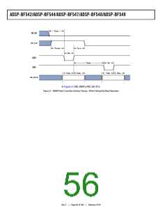
Figure 22. External Port Bus Request and Grant Cycle Timing with Asynchronous BR
Rev. C
|
Page 52 of 100
|
February 2010

 ADI [ ADI ]