ADSP-BF542/ADSP-BF544/ADSP-BF547/ADSP-BF548/ADSP-BF549
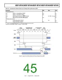
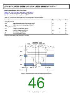
Asynchronous Memory Write Cycle Timing
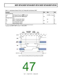
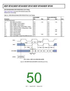
Table 30 and Table 31 on Page 47 and Figure 15 and Figure 16
on Page 47 describe asynchronous memory write cycle opera-
tions for synchronous and for asynchronous ARDY.
Table 30. Asynchronous Memory Write Cycle Timing with Synchronous ARDY
Parameter
Min
Max
Unit
Timing Requirements
tSARDY
tHARDY
Switching Characteristics
ARDY Setup Before the Falling Edge of CLKOUT
5.0
0.0
ns
ns
ARDY Hold After the Falling Edge of CLKOUT
tDDAT
tENDAT
tDO
DATA15–0 Disable After CLKOUT
6.0
6.0
ns
ns
ns
ns
DATA15–0 Enable After CLKOUT
Output Delay After CLKOUT1
Output Hold After CLKOUT1
0.0
0.3
tHO
1 Output pins include AMS3–0, ABE1–0, ADDR19–1, and AWE.
PROGRAMMED ACCESS
SETUP
2 CYCLES
WRITE ACCESS EXTEND HOLD
2 CYCLES
1 CYCLE 1 CYCLE
CLKOUT
AMSx
tDO
tHO
ABE1–0
ADDR19–1
tDO
tHO
AWE
tSARDY tHARDY
ARDY
tHARDY
tENDAT
tSARDY
tDDAT
DATA 15–0
Figure 15. Asynchronous Memory Write Cycle Timing with Synchronous ARDY
Rev. C
|
Page 46 of 100
|
February 2010

 ADI [ ADI ]