ADSP-BF542/ADSP-BF544/ADSP-BF547/ADSP-BF548/ADSP-BF549
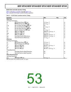
NAND Flash Controller Interface Timing
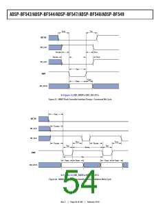
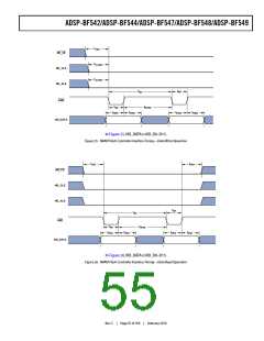
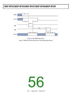
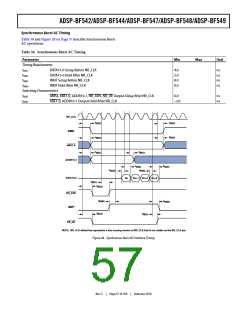
Table 37 and Figure 23 on Page 54 through Figure 27 on
Page 56 describe NAND flash controller interface operations.
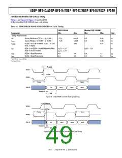
Table 37. NAND Flash Controller Interface Timing
Parameter
Min
Max
Unit
Write Cycle
Switching Characteristics
tCWL
tCH
tCLHWL
tCLH
tALLWL
ND_CE Setup Time to AWE Low
ND_CE Hold Time from AWE High
ND_CLE Setup Time High to AWE Low
ND_CLE Hold Time from AWE High
ND_ALE Setup Time Low to AWE Low
ND_ALE Hold Time from AWE High
AWE Low to AWE High
1.0 × tSCLK – 4
3.0 × tSCLK – 4
0.0
ns
ns
ns
ns
ns
ns
ns
ns
ns
ns
ns
2.5 × tSCLK – 4
0.0
tALH
2.5 × tSCLK – 4
(WR_DLY +1.0) × tSCLK – 4
4.0 × tSCLK – 4
(WR_DLY +5.0) × tSCLK – 4
(WR_DLY +1.5) × tSCLK – 4
2.5 × tSCLK – 4
1
tWP
tWHWL
AWE High to AWE Low
1
tWC
AWE Low to AWE Low
1
tDWS
Data Setup Time for a Write Access
Data Hold Time for a Write Access
tDWH
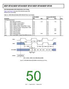
Read Cycle
Switching Characteristics
tCRL
tCRH
ND_CE Setup Time to ARE Low
1.0 × tSCLK – 4
3.0 × tSCLK – 4
(RD_DLY +1.0) × tSCLK – 4
4.0 × tSCLK – 4
(RD_DLY + 5.0) × tSCLK – 4
ns
ns
ns
ns
ns
ND_CE Hold Time from ARE High
ARE Low to ARE High
1
tRP
tRHRL
ARE High to ARE Low
1
tRC
ARE Low to ARE Low
Timing Requirements
tDRS Data Setup Time for a Read Transaction
tDRH Data Hold Time for a Read Transaction
8.0
0.0
ns
ns
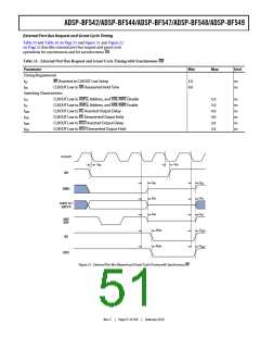
Write Followed by Read
Switching Characteristic
tWHRL
AWE High to ARE Low
5.0 × tSCLK – 4
ns
1 WR_DLY and RD_DLY are defined in the NFC_CTL register.
Rev. C
|
Page 53 of 100
|
February 2010

 ADI [ ADI ]