ADSP-BF542/ADSP-BF544/ADSP-BF547/ADSP-BF548/ADSP-BF549
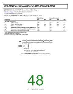
DDR SDRAM/Mobile DDR SDRAM Clock and Control Cycle Timing
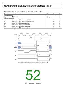
Table 32 and Figure 17 describe DDR SDRAM/mobile DDR
SDRAM clock and control cycle timing.
Table 32. DDR SDRAM/Mobile DDR SDRAM Clock and Control Cycle Timing
DDR SDRAM
Min
Mobile DDR SDRAM
Parameter
Max
Min
Max
Unit
Switching Characteristics
1
tCK
tCH
tCL
DCK0-1 Period
7.50
0.45
0.45
1.00
1.00
2.20
7.50
0.45
0.45
1.00
1.00
2.30
8.33
0.55
0.55
ns
tCK
tCK
ns
ns
ns
DCK0-1 High Pulse Width
0.55
0.55
DCK0-1 Low Pulse Width
2,3
tAS
tAH
Address and Control Output SETUP Time Relative to CK
Address and Control Output HOLD Time Relative to CK
Address and Control Output Pulse Width
2,3
2,3
tOPW
1 The tCK specification does not account for the effects of jitter.
2 Address pins include DA0-12 and DBA0-1.
3 Control pins include DCS0-1, DCLKE, DRAS, DCAS, and DWE.
tCK
tCH
tCL
DCK0-1
tAS
tAH
ADDRESS
CONTROL
tOPW
NOTE: CONTROL = DCS0-1, DCLKE, DRAS, DCAS, AND DWE.
ADDRESS = DA0-12 AND DBA0-1.
Figure 17. DDR SDRAM /Mobile DDR SDRAM Clock and Control Cycle Timing
Rev. C
|
Page 48 of 100
|
February 2010

 ADI [ ADI ]