ADSP-BF542/ADSP-BF544/ADSP-BF547/ADSP-BF548/ADSP-BF549
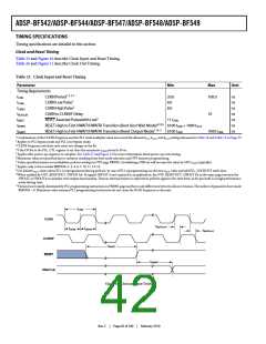
Table 26. Clock Out Timing
Parameter
Min
Max
Unit
Switching Characteristics
tSCLK
CLKOUT Period1,2
7.5
2.5
2.5
ns
ns
ns
tSCLKH
tSCLKL
CLKOUT Width High
CLKOUT Width Low
1 The tSCLK value is the inverse of the fSCLK specification. Reduced supply voltages affect the best-case value of 7.5 ns listed here.
2 The tSCLK value does not account for the effects of jitter.
tSCLK
CLKOUT
tSCLKL
tSCLKH
Figure 11. CLKOUT Interface Timing
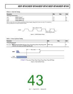
Table 27. Power-Up Reset Timing
Parameter
Min
Max
Unit
Timing Requirements
tRST_IN_PWR RESET Deasserted After the VDDINT, VDDEXT, VDDDDR,VDDUSB,VDDRTC,VDDVR,VDDMP, and 3500 × tCKIN
ns
CLKIN Pins Are Stable and Within Specification
tRST_IN_PWR
RESET
CLKIN
V
DD_SUPPLIES
In Figure 12, VDD_SUPPLIES is VDDINT, VDDEXT, VDDDDR, VDDUSB, VDDRTC, VDDVR, and VDDMP
.
Figure 12. Power-Up Reset Timing
Rev. C
|
Page 43 of 100
|
February 2010

 ADI [ ADI ]