ADSP-BF542/ADSP-BF544/ADSP-BF547/ADSP-BF548/ADSP-BF549
TIMING SPECIFICATIONS
Timing specifications are detailed in this section.
Clock and Reset Timing
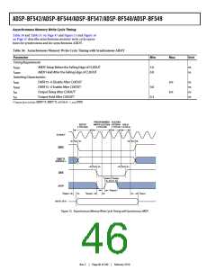
Table 25 and Figure 10 describe Clock Input and Reset Timing.
Table 26 and Figure 11 describe Clock Out Timing.
Table 25. Clock Input and Reset Timing
Parameter
Min
Max
Unit
Timing Requirements
tCKIN
CLKIN Period1, 2, 3, 4
20.0
8.0
100.0
ns
ns
ns
ns
ns
ns
ns
tCKINL
tCKINH
tBUFDLAY
tWRST
CLKIN Low Pulse2
CLKIN High Pulse2
8.0
CLKIN to CLKBUF Delay
RESET Asserted Pulsewidth Low5
RESET High to First HWAIT/HWAITA Transition (Boot Host Wait Mode)6,7,8,9 6100 tCKIN + 7900 tSCLK
RESET High to First HWAIT/HWAITA Transition (Reset Output Mode)7,10,11 6100 tCKIN
10
11 tCKIN
tRHWFT
tRHWFT
7000 tCKIN
1 Combinations of the CLKIN frequency and the PLL clock multiplier must not exceed the allowed fVCO, fCCLK, and fSCLK settings discussed in Table 16 and Table 13 on Page 35.
2 Applies to PLL bypass mode and PLL non-bypass mode.
3 CLKIN frequency and duty cycle must not change on the fly.
4 If the DF bit in the PLL_CTL register is set, then the maximum tCKIN period is 50 ns.
5 Applies after power-up sequence is complete. See Table 27 and Figure 12 for more information about power-up reset timing.
6 Maximum value not specified due to variation resulting from boot mode selection and OTP memory programming.
7 Values specified assume no invalidation preboot settings in OTP page PBS00L. Invalidating a PBS set will increase the value by 1875 tCKIN (typically).
8 Applies only to boot modes BMODE=1, 2, 4, 6, 7, 10, 11, 14, 15.
9 Use default tSCLK value unless PLL is reprogrammed during preboot. In case of PLL reprogramming use the new tSCLK value and add PLL_LOCKCNT settle time.
10When enabled by OTP_RESETOUT_HWAIT bit. If regular HWAIT is not required in an application, the OTP_RESETOUT_HWAIT bit in the same page instructs the
HWAIT or HWAITA to simulate reset output functionality. Then an external resistor is expected to pull the signal to the reset level, as the pin itself is in high performance
mode during reset.
11Variances are mainly dominated by PLL programming instructions in PBS00L page and boot code differences between silicon revisions. The earlier is bypassed in boot mode
BMODE = 0. Maximum value assumes PLL programming instructions do not cause the SCLK frequency to decrease.
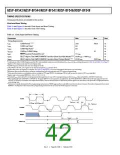
tCKIN
CLKIN
tBUFDLAY
tCKINL
tCKINH
tBUFDLAY
CLKBUF
RESET
tWRST
tRHWFT
HWAIT (A)
Figure 10. Clock and Reset Timing
Rev. C
|
Page 42 of 100
|
February 2010

 ADI [ ADI ]