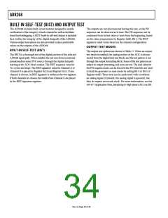
AD9268
External Reference Operation
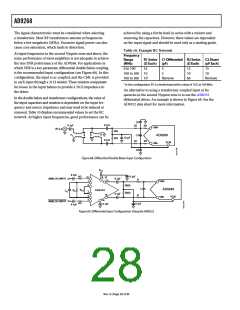
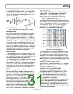
The RF balun configuration is recommended for clock frequencies
between 125 MHz and 625 MHz, and the RF transformer is recom-
mended for clock frequencies from 10 MHz to 200 MHz. The
back-to-back Schottky diodes across the transformer/balun
secondary limit clock excursions into the AD9268 to approx-
imately 0.8 V p-p differential.
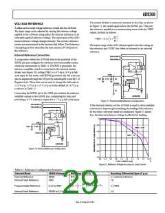
The use of an external reference may be necessary to enhance
the gain accuracy of the ADC or improve thermal drift charac-
teristics. Figure 73 shows the typical drift characteristics of the
internal reference in 1.0 V mode.
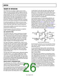
When the SENSE pin is tied to AVDD, the internal reference is
disabled, allowing the use of an external reference. An internal
reference buffer loads the external reference with an equivalent
6 kΩ load (see Figure 62). The internal buffer generates the positive
and negative full-scale references for the ADC core. Therefore,
the external reference must be limited to a maximum of 1.0 V.
2.0
This limit helps prevent the large voltage swings of the clock
from feeding through to other portions of the AD9268 while
preserving the fast rise and fall times of the signal that are critical
to a low jitter performance.
®
Mini-Circuits
ADC
ADT1-1WT, 1:1Z
AD9268
0.1µF
0.1µF
XFMR
CLOCK
INPUT
1.5
CLK+
CLK–
100Ω
VREF = 1.0V
1.0
50Ω
0.1µF
SCHOTTKY
DIODES:
HSMS2822
0.5
0
0.1µF
Figure 75. Transformer-Coupled Differential Clock (Up to 200 MHz)
–0.5
–1.0
ADC
AD9268
1nF
50Ω
1nF
0.1µF
0.1µF
CLOCK
INPUT
CLK+
–1.5
–2.0
CLK–
–40
–20
0
20
40
60
80
TEMPERATURE (°C)
SCHOTTKY
DIODES:
HSMS2822
Figure 73. Typical VREF Drift
Figure 76. Balun-Coupled Differential Clock (Up to 625 MHz)
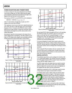
CLOCK INPUT CONSIDERATIONS
If a low jitter clock source is not available, another option is to
ac couple a differential PECL signal to the sample clock input
pins, as shown in Figure 77. The AD9510/AD9511/AD9512/
AD9513/AD9514/AD9515/AD9516/AD9517/AD9518 clock
drivers offer excellent jitter performance.
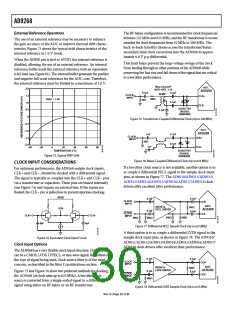
For optimum performance, the AD9268 sample clock inputs,
CLK+ and CLK−, should be clocked with a differential signal.
The signal is typically ac-coupled into the CLK+ and CLK− pins
via a transformer or capacitors. These pins are biased internally
(see Figure 74) and require no external bias. If the inputs are
floated, the CLK− pin is pulled low to prevent spurious clocking.
AVDD
0.1µF
0.1µF
CLOCK
INPUT
CLK+
ADC
AD9268
AD951x
PECL DRIVER
100Ω
0.9V
0.1µF
0.1µF
CLOCK
INPUT
CLK–
CLK+
CLK–
240Ω
240Ω
50kΩ
50kΩ
4pF
4pF
Figure 77. Differential PECL Sample Clock (Up to 625 MHz)
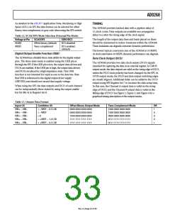
A third option is to ac couple a differential LVDS signal to the
sample clock input pins, as shown in Figure 78. The AD9510/
AD9511/AD9512/AD9513/AD9514/AD9515/AD9516/AD9517/
AD9518 clock drivers offer excellent jitter performance.
Figure 74. Equivalent Clock Input Circuit
Clock Input Options
The AD9268 has a very flexible clock input structure. Clock input
can be a CMOS, LVDS, LVPECL, or sine wave signal. Regardless of
the type of signal being used, clock source jitter is of the most
concern, as described in the Jitter Considerations section.
0.1µF
0.1µF
CLOCK
INPUT
CLK+
ADC
AD9268
AD951x
LVDS DRIVER
100Ω
0.1µF
Figure 75 and Figure 76 show two preferred methods for clocking
the AD9268 (at clock rates up to 625 MHz). A low jitter clock
source is converted from a single-ended signal to a differential
signal using either an RF balun or an RF transformer.
0.1µF
CLOCK
INPUT
CLK–
50kΩ
50kΩ
Figure 78. Differential LVDS Sample Clock (Up to 625 MHz)
Rev. A | Page 3± of 44

 ADI [ ADI ]