AD9268
THEORY OF OPERATION
A small resistor in series with each input can help reduce the
peak transient current required from the output stage of the
driving source. A shunt capacitor can be placed across the inputs
to provide dynamic charging currents. This passive network
creates a low-pass filter at the ADC input; therefore, the precise
values are dependent on the application.
The AD9268 dual-core analog-to-digital converter (ADC)
design can be used for diversity reception of signals, in which the
ADCs are operating identically on the same carrier but from two
separate antennae. The ADCs can also be operated with inde-
pendent analog inputs. The user can sample any fS/2 frequency
segment from dc to 200 MHz, using appropriate low-pass or
band-pass filtering at the ADC inputs with little loss in ADC
performance. Operation to 300 MHz analog input is permitted,
but it occurs at the expense of increased ADC noise and distortion.
In intermediate frequency (IF) undersampling applications, any
shunt capacitors should be reduced. In combination with the
driving source impedance, the shunt capacitors limit the input
bandwidth. Refer to the AN-742 Application Note, Frequency
Domain Response of Switched-Capacitor ADCs; the AN-827
Application Note, A Resonant Approach to Interfacing Amplifiers to
Switched-Capacitor ADCs; and the Analog Dialogue article,
“Transformer-Coupled Front-End for Wideband A/D Converters,”
for more information on this subject (refer to www.analog.com).
BIAS
In nondiversity applications, the AD9268 can be used as a base-
band or direct downconversion receiver, in which one ADC is
used for I input data, and the other is used for Q input data.
Synchronization capability is provided to allow synchronized
timing between multiple devices.
Programming and control of the AD9268 are accomplished
using a 3-wire SPI-compatible serial interface.
S
S
C
FB
C
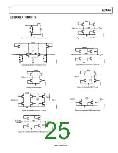
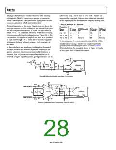
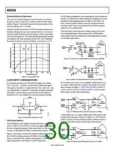
ADC ARCHITECTURE
S
VIN+
The AD9268 architecture consists of a dual front-end sample-
and-hold circuit, followed by a pipelined, switched-capacitor
ADC. The quantized outputs from each stage are combined into
a final 16-bit result in the digital correction logic. The pipelined
architecture permits the first stage to operate on a new input
sample and the remaining stages to operate on the preceding
samples. Sampling occurs on the rising edge of the clock.
C
PAR1
C
PAR2
H
S
S
S
C
S
VIN–
C
FB
C
C
PAR1
PAR2
S
BIAS
Figure 64. Switched-Capacitor Input
Each stage of the pipeline, excluding the last, consists of a low
resolution flash ADC connected to a switched-capacitor digital-
to-analog converter (DAC) and an interstage residue amplifier
(MDAC). The MDAC magnifies the difference between the
reconstructed DAC output and the flash input for the next stage
in the pipeline. One bit of redundancy is used in each stage to
facilitate digital correction of flash errors. The last stage simply
consists of a flash ADC.
For best dynamic performance, the source impedances driving
VIN+ and VIN− should be matched, and the inputs should be
differentially balanced.
An internal differential reference buffer creates positive and
negative reference voltages that define the input span of the ADC
core. The span of the ADC core is set by this buffer to 2 × VREF.
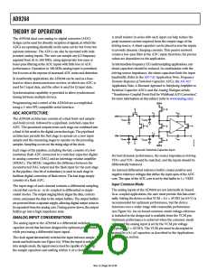
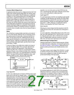
Input Common Mode
The input stage of each channel contains a differential sampling
circuit that can be ac- or dc-coupled in differential or single-
ended modes. The output staging block aligns the data, corrects
errors, and passes the data to the output buffers. The output buffers
are powered from a separate supply, allowing digital output noise to
be separated from the analog core. During power-down, the output
buffers go into a high impedance state.
The analog inputs of the AD9268 are not internally dc biased.
In ac-coupled applications, the user must provide this bias exter-
nally. Setting the device so that VCM = 0.5 × AVDD (or 0.9 V) is
recommended for optimum performance, but the device
functions over a wider range with reasonable performance
(see Figure 54). An on-board common-mode voltage reference
is included in the design and is available from the VCM pin.
Optimum performance is achieved when the common-mode
voltage of the analog input is set by the VCM pin voltage
(typically 0.5 × AVDD). The VCM pin must be decoupled to
ground by a 0.1 μF capacitor, as described in the Applications
Information section.
ANALOG INPUT CONSIDERATIONS
The analog input to the AD9268 is a differential switched-
capacitor circuit that has been designed for optimum performance
while processing a differential input signal.
The clock signal alternatively switches the input between sample
mode and hold mode (see Figure 64). When the input is switched
into sample mode, the signal source must be capable of charging
the sample capacitors and settling within ½ of a clock cycle.
Rev. A | Page 26 of 44

 ADI [ ADI ]